Patented Manufacturing Processes in IGZO Thin Film Production
SEP 28, 20259 MIN READ
Generate Your Research Report Instantly with AI Agent
Patsnap Eureka helps you evaluate technical feasibility & market potential.
IGZO Thin Film Technology Evolution and Objectives
Indium Gallium Zinc Oxide (IGZO) thin film technology has evolved significantly since its initial development in the early 2000s. The journey began with Hosono's research group at Tokyo Institute of Technology, who first demonstrated the potential of amorphous oxide semiconductors with high electron mobility. This breakthrough laid the foundation for IGZO's application in display technologies, offering superior performance compared to conventional amorphous silicon (a-Si) thin film transistors.
The evolution of IGZO thin film technology has been marked by continuous improvements in deposition techniques, from early radio frequency (RF) magnetron sputtering to more advanced methods including pulsed laser deposition (PLD) and atomic layer deposition (ALD). Each advancement has contributed to enhanced film quality, uniformity, and electrical properties, enabling the expansion of IGZO applications beyond displays to sensors, memory devices, and flexible electronics.
Manufacturing processes for IGZO thin films have undergone significant refinement, with patented innovations addressing key challenges in stoichiometry control, defect management, and interface engineering. Notable milestones include Sharp Corporation's commercialization of IGZO displays in 2012, followed by LG Display and Samsung's entry into the market with their proprietary manufacturing processes, each protected by extensive patent portfolios.
The technical objectives driving IGZO thin film development have evolved from basic feasibility demonstrations to addressing specific manufacturing challenges. Current objectives focus on enhancing carrier mobility while maintaining low off-state current, improving stability under environmental stresses, and developing low-temperature processes compatible with flexible substrates. These objectives align with industry demands for higher resolution, lower power consumption displays, and emerging applications in wearable and foldable electronics.
Patent landscapes reveal concentrated efforts in optimizing sputtering parameters, post-deposition treatments, and multi-layer structures to enhance device performance. Companies like Sharp, Samsung, LG Display, and research institutions like KAIST have established strong intellectual property positions in specialized manufacturing techniques that yield IGZO films with superior electrical characteristics and stability.
Looking forward, the technology trajectory points toward integration with emerging display technologies such as microLED and OLED, as well as expansion into new application domains including transparent electronics and neuromorphic computing. The objectives now extend beyond performance metrics to include sustainability considerations, with research focusing on reducing rare metal content and developing environmentally friendly manufacturing processes.
Market Analysis for IGZO Display Applications
The IGZO (Indium Gallium Zinc Oxide) display market has experienced significant growth over the past decade, driven primarily by increasing demand for high-resolution, energy-efficient displays across multiple device categories. The global IGZO display market was valued at approximately $11.2 billion in 2022 and is projected to reach $23.5 billion by 2028, representing a compound annual growth rate (CAGR) of 13.2% during the forecast period.
Mobile devices constitute the largest application segment for IGZO displays, accounting for roughly 45% of the total market share. This dominance stems from IGZO's ability to deliver higher pixel densities while consuming significantly less power than traditional amorphous silicon (a-Si) displays, extending battery life in smartphones and tablets. Apple has been a major adopter, incorporating IGZO technology in various iPad and iPhone models since 2012.
The television segment represents the second-largest application area, with approximately 30% market share. Premium OLED and QLED TVs increasingly utilize IGZO backplanes to achieve superior refresh rates and power efficiency. Major manufacturers including Samsung, LG, and Sony have integrated IGZO technology into their high-end television lineups.
Commercial displays and monitors comprise about 15% of the market, with growing adoption in professional-grade monitors for design, video editing, and medical imaging applications where color accuracy and resolution are critical. The remaining 10% encompasses emerging applications including automotive displays, wearable devices, and industrial control panels.
Regionally, East Asia dominates IGZO display production and consumption, with Japan, South Korea, Taiwan, and China collectively accounting for over 70% of global market value. North America and Europe represent significant consumption markets but have limited production capacity.
Key market drivers include increasing consumer preference for high-resolution displays, growing adoption of OLED technology (which often utilizes IGZO backplanes), and expanding applications in automotive and medical sectors. The rising demand for foldable and flexible displays also favors IGZO technology due to its compatibility with flexible substrates.
Market challenges include high initial manufacturing costs compared to conventional a-Si technology, technical complexities in scaling production, and competition from alternative technologies such as LTPS (Low-Temperature Polysilicon). Additionally, supply chain vulnerabilities exist due to the limited availability of indium, a critical raw material for IGZO production.
IGZO Manufacturing Challenges and Global Development Status
The global IGZO (Indium Gallium Zinc Oxide) thin film manufacturing landscape presents significant technical challenges that have shaped its development trajectory. Currently, the production of high-quality IGZO films faces several critical hurdles, including composition control, uniformity across large substrates, and defect management during deposition processes. These challenges are particularly pronounced when scaling to Generation 8 and larger substrates used in modern display manufacturing.
Manufacturing stability remains a persistent issue, with process parameter sensitivity requiring precise control of sputtering conditions, including pressure, power, and gas flow rates. Even minor deviations can result in significant variations in electrical properties, affecting device performance and yield rates. This sensitivity has created a technological barrier that separates industry leaders from followers.
Geographically, IGZO manufacturing expertise is concentrated in East Asia, with Japan, South Korea, and Taiwan leading development efforts. Japanese companies, particularly Sharp Corporation (now part of Foxconn) and SEL (Semiconductor Energy Laboratory), hold foundational patents in IGZO technology. South Korean giants Samsung and LG Display have developed proprietary manufacturing processes, while Taiwanese firms like AUO and Innolux have established competitive production capabilities.
In the United States and Europe, research institutions rather than commercial manufacturers dominate the IGZO development landscape. Companies like Applied Materials and Canon Anelva have focused on equipment development rather than direct film production, creating specialized deposition systems optimized for IGZO materials.
China has rapidly expanded its IGZO manufacturing capacity, with BOE Technology and CSOT making significant investments in recent years. However, these manufacturers still face challenges in achieving the highest performance metrics and often rely on licensed technology or equipment from Japanese or American suppliers.
The technical maturity of IGZO manufacturing varies significantly by application. While processes for LCD backplanes have reached commercial maturity, manufacturing techniques for more demanding applications such as OLED backplanes and transparent electronics remain in development phases. The yield rates for advanced applications can be 15-30% lower than those for standard LCD implementations.
Recent advancements in co-sputtering techniques and multi-chamber deposition systems have addressed some uniformity challenges, but issues related to oxygen vacancy control and interface quality continue to limit performance in high-end applications. The industry has responded by developing specialized post-deposition treatments, including precisely controlled annealing processes and passivation techniques, which have become critical differentiators in manufacturing capability.
Current Patented IGZO Manufacturing Methodologies
01 IGZO thin film composition and structure
Indium Gallium Zinc Oxide (IGZO) thin films are composed of specific ratios of indium, gallium, zinc, and oxygen. The composition and structure of these films significantly affect their electrical and optical properties. Various deposition techniques and post-treatment processes can be employed to optimize the crystallinity, density, and uniformity of IGZO thin films, which are crucial for their performance in electronic devices.- IGZO thin film fabrication methods: Various methods for fabricating Indium Gallium Zinc Oxide (IGZO) thin films have been developed to optimize their electrical and physical properties. These methods include sputtering, chemical vapor deposition, and solution-based processes. The fabrication parameters such as temperature, pressure, and gas flow rates significantly affect the crystallinity, density, and performance of the resulting IGZO films. Advanced techniques allow for precise control of film thickness and composition, which are critical for semiconductor device applications.
- IGZO thin film transistor (TFT) structures: IGZO thin film transistors feature various structural designs to enhance performance characteristics. These structures include bottom-gate, top-gate, and dual-gate configurations, each offering different advantages in terms of mobility, stability, and threshold voltage control. The channel layer thickness, gate dielectric materials, and electrode configurations significantly impact the TFT performance. Novel structures incorporate additional layers or treatments to improve stability against environmental factors and reduce defects at interfaces.
- IGZO thin film doping and composition optimization: The electrical properties of IGZO thin films can be significantly enhanced through doping and composition optimization. By adjusting the ratio of indium, gallium, and zinc, or by introducing dopants such as hydrogen, nitrogen, or metal elements, the carrier concentration, mobility, and stability can be controlled. Composition engineering helps reduce oxygen vacancies, which are major defects in IGZO films. These modifications enable customization of IGZO properties for specific applications, from high-performance displays to low-power electronics.
- IGZO thin film applications in display technology: IGZO thin films have revolutionized display technology due to their high electron mobility and transparency. They are widely used in active-matrix displays, including OLED and LCD panels, enabling higher resolution, faster refresh rates, and lower power consumption. The superior switching characteristics of IGZO TFTs allow for smaller pixel sizes and narrower bezels in displays. Additionally, IGZO technology enables the development of flexible, transparent, and large-area displays with improved image quality and energy efficiency.
- IGZO thin film post-treatment and stability enhancement: Post-deposition treatments are crucial for enhancing the stability and performance of IGZO thin films. These treatments include thermal annealing, plasma treatment, passivation layer deposition, and surface modification techniques. Such processes help reduce defects, stabilize the film structure, and improve resistance to environmental factors like humidity and light. Advanced passivation techniques using inorganic or organic materials protect IGZO films from degradation during operation, extending device lifetime and maintaining consistent performance under various operating conditions.
02 IGZO thin film transistor (TFT) fabrication methods
Fabrication methods for IGZO thin film transistors involve specific deposition techniques such as sputtering, chemical vapor deposition, or solution processing. These methods include precise control of process parameters like temperature, pressure, and gas flow rates. Post-deposition treatments such as annealing in different atmospheres can significantly improve the electrical characteristics of IGZO TFTs, enhancing their mobility, stability, and threshold voltage characteristics.Expand Specific Solutions03 IGZO thin film applications in display technology
IGZO thin films are widely used in display technologies due to their high electron mobility and transparency. They serve as the active layer in thin film transistors for LCD and OLED displays, enabling higher resolution, faster response times, and lower power consumption compared to conventional amorphous silicon. The implementation of IGZO in display backplanes allows for the development of flexible, transparent, and high-performance display panels.Expand Specific Solutions04 IGZO thin film defect control and stability enhancement
Controlling defects and enhancing stability in IGZO thin films involves managing oxygen vacancies, which significantly affect electrical properties. Various techniques are employed to reduce defects, including optimized deposition parameters, specific annealing processes, and passivation layers. Stability enhancement methods address issues like negative bias temperature instability and light-induced degradation, which are critical for long-term device performance in various environmental conditions.Expand Specific Solutions05 IGZO thin film integration with other materials and structures
Integration of IGZO thin films with other materials and structures involves creating multilayer systems for enhanced functionality. This includes combining IGZO with various dielectric materials, electrodes, and other semiconductors to create complex device architectures. Such integration enables the development of advanced electronic devices like sensors, memory elements, and integrated circuits with improved performance characteristics, while addressing interface issues and compatibility challenges.Expand Specific Solutions
Leading Companies in IGZO Patent Landscape
The IGZO thin film production market is currently in a growth phase, characterized by increasing demand for high-performance displays across consumer electronics. The market size is expanding rapidly, driven by applications in smartphones, tablets, and large-format displays, with projections exceeding $5 billion by 2025. Regarding technical maturity, major players like Samsung Display, LG Display, and BOE Technology have established advanced patented manufacturing processes, while Sharp and Canon hold foundational patents in IGZO technology. Chinese manufacturers including TCL China Star Optoelectronics and Shenzhen China Star Optoelectronics are rapidly closing the technology gap through significant R&D investments. Applied Materials and Tokyo Electron provide critical equipment solutions, creating a competitive ecosystem where intellectual property protection increasingly determines market advantage.
LG Display Co., Ltd.
Technical Solution: LG Display has developed advanced IGZO thin film manufacturing processes focused on large-area applications. Their patented approach incorporates a modified co-sputtering technique that allows precise control of the metal oxide composition during deposition. LG's process features a distinctive two-step annealing method that first establishes the basic crystalline structure, followed by a specialized hydrogen passivation treatment to reduce defect states. The company has patented a unique electrode configuration for their sputtering systems that improves uniformity across large substrates, critical for their focus on television and premium display markets. LG Display's manufacturing process also includes proprietary encapsulation techniques that protect IGZO layers from moisture and oxygen degradation, extending device lifetime. Their patented methods address common IGZO challenges such as threshold voltage instability through carefully engineered buffer layers and interface treatments between the semiconductor and dielectric layers. LG has integrated these processes into their production lines for high-end OLED and LCD displays requiring thin film transistor backplanes.
Strengths: Excellent uniformity across large substrates, enabling consistent performance in large displays. Advanced encapsulation technology providing superior environmental stability and longer device lifetime. Weaknesses: Complex multi-step process requiring sophisticated equipment and precise control, resulting in higher production costs and potential yield challenges during scale-up.
BOE Technology Group Co., Ltd.
Technical Solution: BOE Technology has developed comprehensive patented manufacturing processes for IGZO thin film production focused on high-volume applications. Their approach centers on a modified pulsed DC magnetron sputtering technique that achieves high deposition rates while maintaining film quality. BOE's patents cover specialized target compositions with proprietary dopants that enhance carrier concentration and stability. Their manufacturing process incorporates a unique low-temperature annealing sequence that minimizes substrate warping while optimizing semiconductor performance. BOE has patented a multi-layer structure that includes carefully engineered buffer and passivation layers to protect the IGZO channel and improve device reliability. Their process innovations extend to specialized etching techniques that create precise channel geometries with minimal undercut, improving transistor performance and yield. BOE has also developed automated optical inspection systems specifically calibrated for IGZO defect detection, integrated directly into their production lines. These manufacturing advances have enabled BOE to implement IGZO technology across various display products, from smartphones to large-format displays.
Strengths: High-volume production capability with excellent cost efficiency through optimized processes and equipment utilization. Comprehensive quality control systems specifically designed for IGZO manufacturing. Weaknesses: Relatively newer to IGZO technology compared to Japanese pioneers, with potentially less fundamental IP in core material science aspects. Some dependence on equipment suppliers for key process technologies.
Critical Patent Analysis for IGZO Thin Film Production
Method for producing a-IGZO oxide thin film
PatentActiveUS8148245B2
Innovation
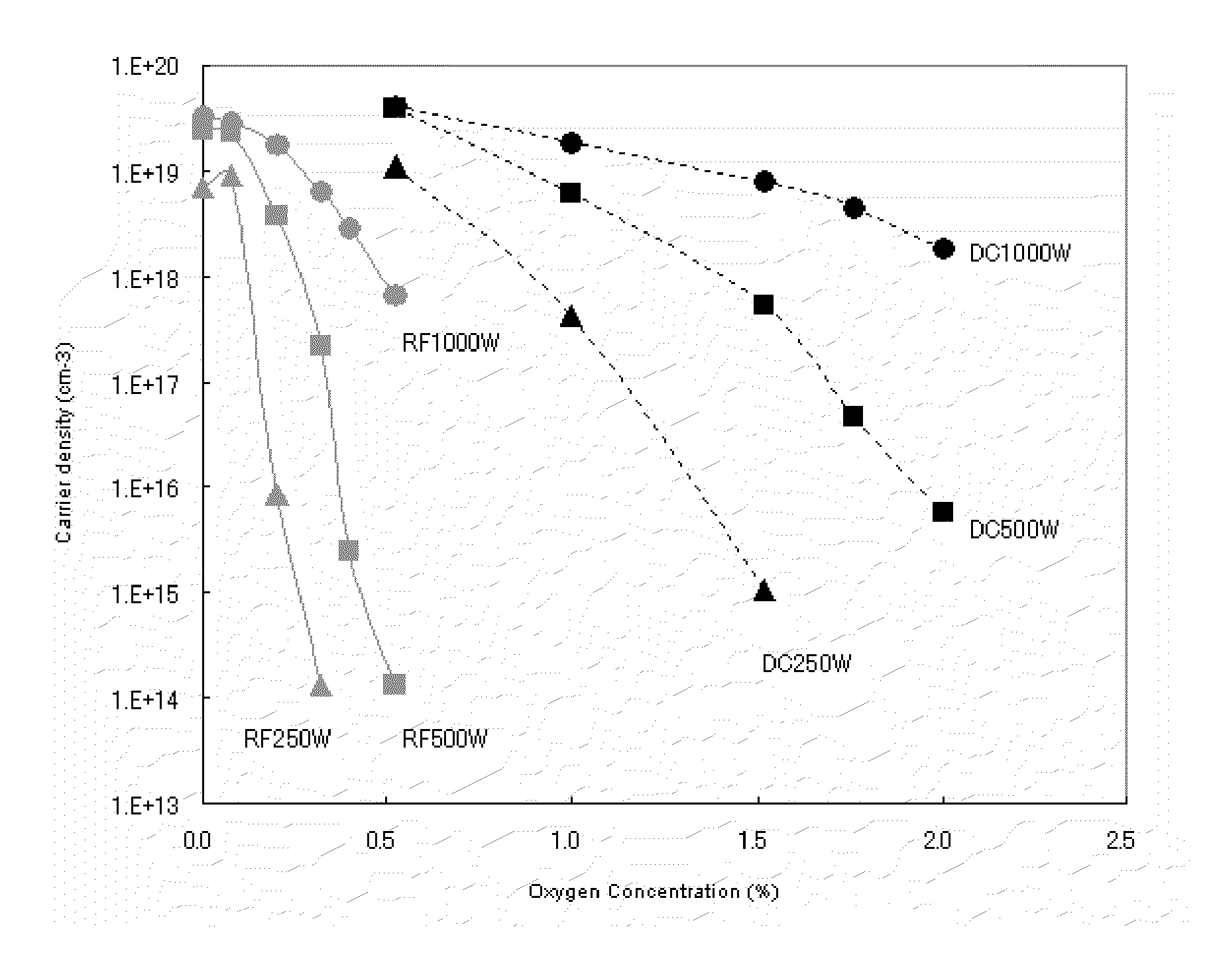
- A method involving direct current sputtering with a sintered oxide target of indium, gallium, and zinc, optimized with specific composition ratios and resistance, and subsequent annealing in an oxygen-rich atmosphere to stabilize carrier density, allowing for high reproducibility and suitable for large-area deposition.
Process for producing thin film of a-IGZO oxide
PatentWO2009084537A1
Innovation
- The use of a DC sputtering method with increased sputtering power density and an oxide sintered body with specific atomic ratios of indium, gallium, and zinc, along with post-deposition annealing in an oxygen-rich atmosphere, allows for precise control of carrier concentration and improved film quality.
Intellectual Property Strategy for IGZO Technology
The intellectual property landscape surrounding IGZO (Indium Gallium Zinc Oxide) technology represents a critical strategic consideration for companies operating in this space. Patent protection for manufacturing processes has become increasingly important as IGZO thin film technology gains wider adoption in display and semiconductor industries.
Major technology companies have established comprehensive patent portfolios covering various aspects of IGZO manufacturing. Sharp Corporation holds foundational patents related to IGZO composition and basic manufacturing techniques, having been an early pioneer in the field. Samsung and LG Display have developed extensive patent portfolios focusing on process optimization for large-scale production, while companies like Applied Materials and Tokyo Electron have secured intellectual property rights for specialized deposition equipment.
Strategic patent mapping reveals several key areas of protection: material composition formulations, deposition techniques (particularly sputtering parameters), annealing processes, and interface engineering between IGZO and adjacent layers. The geographical distribution of patents shows concentration in Japan, South Korea, Taiwan, and increasingly China, reflecting the manufacturing centers for display technologies.
Cross-licensing agreements have become common practice in the industry, with major players establishing strategic partnerships to navigate the complex patent landscape. For example, Sharp has entered licensing agreements with multiple display manufacturers to monetize their foundational IGZO patents while gaining access to complementary technologies.
For companies entering the IGZO space, several IP strategies merit consideration. Defensive patenting around specific manufacturing improvements can create negotiating leverage, even for organizations lacking foundational patents. Freedom-to-operate analyses should be conducted regularly, particularly focusing on process parameters that may inadvertently infringe existing patents during scale-up.
Patent monitoring systems should be implemented to track new filings in the IGZO space, particularly those related to manufacturing process improvements. This enables early identification of emerging competitors and potential infringement risks. Companies should also consider strategic patent acquisitions to strengthen their position, particularly focusing on process-specific improvements that can be implemented without major capital investment.
The development of trade secrets as a complementary strategy to patent protection is also valuable, particularly for process optimizations that are difficult to detect through product analysis. This hybrid approach provides longer-term protection for manufacturing know-how while still establishing formal IP rights for detectable innovations.
Environmental Impact of IGZO Manufacturing Processes
The manufacturing of IGZO (Indium Gallium Zinc Oxide) thin films presents significant environmental considerations that warrant careful examination. Traditional semiconductor manufacturing processes are known for their substantial environmental footprint, including high energy consumption, water usage, and hazardous chemical utilization. IGZO production, while offering advantages in certain areas, still poses environmental challenges that must be addressed.
Primary environmental concerns in IGZO manufacturing include the use of rare metals, particularly indium, which faces supply constraints and environmentally problematic extraction methods. The sputtering processes commonly employed in patented IGZO manufacturing techniques require substantial energy inputs, contributing to carbon emissions when powered by non-renewable energy sources. Additionally, the etching and cleaning phases utilize various chemicals that may present disposal challenges and potential environmental hazards if not properly managed.
Several patented IGZO manufacturing processes have incorporated environmentally conscious innovations. For instance, patents by Sharp Corporation and Samsung have introduced low-temperature deposition techniques that significantly reduce energy consumption compared to conventional methods. These approaches not only decrease the carbon footprint but also extend equipment lifespan, reducing manufacturing waste. Other patents focus on reducing chemical usage through optimized deposition parameters and alternative precursor materials.
Water consumption represents another critical environmental factor in IGZO production. Conventional semiconductor manufacturing can require thousands of liters of ultra-pure water per wafer. Recent patented processes have implemented closed-loop water recycling systems and dry etching techniques that substantially reduce water requirements. These innovations align with growing regulatory pressures and industry sustainability initiatives.
Waste management challenges persist in IGZO manufacturing. The industry generates both solid waste (including target materials and substrates) and liquid waste streams containing heavy metals and process chemicals. Several patented approaches address this through material reclamation systems that recover valuable metals from waste streams, reducing both environmental impact and production costs. Additionally, some manufacturers have developed non-toxic alternative chemicals for cleaning and etching processes.
Life cycle assessments of patented IGZO manufacturing processes reveal varying environmental impacts depending on specific implementation details. When compared to traditional amorphous silicon or LTPS (Low-Temperature Polysilicon) processes, IGZO manufacturing generally demonstrates lower lifetime environmental impact due to reduced operating temperatures and fewer process steps, despite the initial concerns regarding rare metal usage.
Unlock deeper insights with Patsnap Eureka Quick Research — get a full tech report to explore trends and direct your research. Try now!
Generate Your Research Report Instantly with AI Agent
Supercharge your innovation with Patsnap Eureka AI Agent Platform!