IGZO Thin Film and its Role in Energy Harvesting Systems
SEP 28, 202510 MIN READ
Generate Your Research Report Instantly with AI Agent
Patsnap Eureka helps you evaluate technical feasibility & market potential.
IGZO Technology Background and Energy Harvesting Goals
Indium Gallium Zinc Oxide (IGZO) thin film technology represents a significant advancement in semiconductor materials, emerging in the early 2000s as a promising alternative to amorphous silicon. Initially developed by researchers at Tokyo Institute of Technology and later commercialized by companies like Sharp Corporation, IGZO combines the transparency of zinc oxide with the stability and performance characteristics provided by indium and gallium. This unique composition results in exceptional electron mobility—10 to 50 times higher than amorphous silicon—while maintaining transparency and enabling low-power operation.
The evolution of IGZO technology has been marked by continuous improvements in deposition techniques, from early radio frequency sputtering methods to more sophisticated approaches including pulsed laser deposition and solution-based processes. These advancements have progressively enhanced film quality, uniformity, and production scalability, making IGZO increasingly viable for commercial applications beyond its initial use in display technologies.
In recent years, IGZO has attracted significant attention for its potential role in energy harvesting systems, representing a convergence of semiconductor technology with sustainable energy solutions. This interest stems from IGZO's unique combination of properties: high electron mobility, optical transparency, mechanical flexibility, and low-temperature processing compatibility. These characteristics make it particularly suitable for integration into various energy harvesting devices, including photovoltaics, piezoelectric systems, and thermoelectric generators.
The primary technical goal in IGZO-based energy harvesting research is to develop highly efficient, cost-effective, and environmentally sustainable systems capable of converting ambient energy sources into usable electrical power. Specific objectives include enhancing the power conversion efficiency of IGZO-based photovoltaic cells, improving the sensitivity and response of IGZO-integrated piezoelectric harvesters, and optimizing the thermoelectric properties of IGZO-based materials for temperature gradient energy capture.
Another critical goal involves developing IGZO thin films with enhanced stability under various environmental conditions, including humidity, temperature fluctuations, and mechanical stress. This stability is essential for ensuring the long-term reliability of energy harvesting systems deployed in real-world applications, from building-integrated photovoltaics to wearable electronics powered by body heat or motion.
The integration of IGZO with other emerging technologies, such as flexible electronics and Internet of Things (IoT) devices, represents another important technical direction. Researchers aim to create self-powered systems where IGZO serves dual functions—as both an active semiconductor component in electronic circuits and as part of the energy harvesting mechanism that powers those same circuits.
Market Analysis for IGZO-Based Energy Harvesting Solutions
The global market for IGZO-based energy harvesting solutions is experiencing significant growth, driven by the increasing demand for sustainable energy sources and the proliferation of IoT devices. The market size for energy harvesting systems was valued at approximately $440 million in 2020 and is projected to reach $1.3 billion by 2028, representing a CAGR of 13.2% during the forecast period. IGZO thin film technology is positioned to capture a substantial portion of this market due to its unique properties and versatility.
Consumer electronics represents the largest application segment for IGZO-based energy harvesting solutions, accounting for nearly 35% of the market share. This dominance is attributed to the growing adoption of wearable devices, smartphones, and tablets that benefit from IGZO's high electron mobility and transparency characteristics. The healthcare sector follows closely, with applications in medical wearables and remote patient monitoring systems driving demand.
Geographically, Asia Pacific leads the market with approximately 40% share, primarily due to the strong presence of electronics manufacturers in countries like Japan, South Korea, and Taiwan. Companies such as Sharp Corporation and Samsung Electronics have made significant investments in IGZO technology development. North America and Europe collectively account for about 45% of the market, with increasing adoption in smart building applications and industrial automation.
The market is segmented by energy source, with solar being the predominant harvesting method compatible with IGZO thin films, followed by thermal, vibration, and RF energy harvesting. Solar-based solutions represent approximately 50% of the IGZO energy harvesting market due to the excellent light absorption properties of IGZO materials when properly engineered.
Key market drivers include the growing emphasis on energy efficiency, the miniaturization of electronic devices, and increasing investments in smart infrastructure. The push toward carbon neutrality and sustainable energy solutions has created favorable regulatory environments in many regions, further stimulating market growth.
Challenges affecting market expansion include high initial production costs, technical limitations in energy conversion efficiency, and competition from alternative technologies such as organic photovoltaics and perovskite solar cells. However, ongoing research and development efforts are gradually addressing these barriers, improving the commercial viability of IGZO-based energy harvesting solutions.
The market is characterized by strategic partnerships between material manufacturers, device makers, and end-users to create integrated energy harvesting ecosystems. This collaborative approach is accelerating commercialization and expanding application possibilities across various industries.
IGZO Thin Film Development Status and Technical Barriers
IGZO (Indium Gallium Zinc Oxide) thin film technology has emerged as a significant advancement in semiconductor materials, particularly for transparent electronics and energy harvesting applications. Currently, IGZO thin films are predominantly manufactured using physical vapor deposition methods, with RF magnetron sputtering being the most widely adopted industrial technique due to its scalability and film quality consistency. Alternative methods such as pulsed laser deposition and solution processing are gaining research attention but remain limited to laboratory settings.
The global landscape of IGZO technology development shows concentration in East Asia, particularly Japan, South Korea, and Taiwan, where major display manufacturers have established significant intellectual property portfolios. European and North American research institutions focus more on fundamental material science aspects and novel applications beyond displays.
Despite its promising properties, IGZO thin film technology faces several critical technical barriers. The most significant challenge remains the stability of electrical properties under environmental stressors. IGZO films exhibit sensitivity to oxygen and moisture, resulting in threshold voltage shifts and carrier mobility degradation over time. This instability is particularly problematic for energy harvesting applications where long-term reliability is essential.
Another major technical hurdle is the trade-off between transparency and conductivity. While IGZO offers superior electron mobility compared to amorphous silicon, achieving the optimal balance between optical transparency and electrical performance remains challenging, especially when targeting high-efficiency energy harvesting systems that require both properties simultaneously.
The deposition temperature dependency presents another barrier, as high-quality IGZO films typically require temperatures above 200°C for optimal performance. This thermal requirement limits compatibility with flexible substrates and increases manufacturing costs, hindering widespread adoption in next-generation flexible energy harvesting devices.
Interface engineering represents a persistent challenge, as the performance of IGZO-based devices is heavily influenced by the quality of interfaces with adjacent layers. Controlling defect states and charge trapping at these interfaces remains difficult to standardize across different device architectures and manufacturing processes.
Scaling production while maintaining performance consistency presents significant industrial challenges. Variations in film thickness, composition, and microstructure across large substrates affect device-to-device uniformity, a critical factor for commercial viability of energy harvesting arrays.
Recent research has begun addressing these barriers through approaches such as passivation layers, compositional tuning, and post-deposition treatments. However, a comprehensive solution that simultaneously addresses stability, performance, and manufacturing scalability remains elusive, indicating substantial room for innovation in this field.
Current IGZO Implementation in Energy Harvesting Applications
01 IGZO thin film fabrication methods
Various methods for fabricating Indium Gallium Zinc Oxide (IGZO) thin films are disclosed, including sputtering, chemical vapor deposition, and solution processing techniques. These methods focus on controlling the deposition parameters to achieve optimal film quality, uniformity, and electrical properties. The fabrication processes often involve specific temperature controls, gas flow rates, and post-deposition treatments to enhance the performance of the resulting IGZO thin films.- Composition and structure of IGZO thin films: IGZO (Indium Gallium Zinc Oxide) thin films are semiconductor materials composed of indium, gallium, zinc, and oxygen. The composition ratio of these elements significantly affects the electrical properties of the film. Various deposition techniques such as sputtering, atomic layer deposition, and solution processing are used to create these films with specific structural characteristics. The crystalline structure, thickness, and uniformity of IGZO films are critical factors that determine their performance in electronic devices.
- IGZO thin film transistor fabrication and optimization: The fabrication of IGZO thin film transistors (TFTs) involves multiple steps including substrate preparation, film deposition, patterning, and annealing processes. Various optimization techniques are employed to enhance transistor performance, such as controlling the channel thickness, optimizing the gate dielectric interface, and implementing specific annealing protocols. These optimizations aim to improve carrier mobility, threshold voltage stability, and overall device reliability for applications in display technologies and flexible electronics.
- Defect control and stability enhancement in IGZO films: Controlling defects in IGZO thin films is crucial for device performance and stability. Various methods are employed to reduce oxygen vacancies and other defects, including post-deposition treatments, passivation layers, and doping strategies. Environmental stability is enhanced through protective coatings and encapsulation techniques that shield the IGZO layer from moisture and oxygen. These approaches significantly improve the long-term reliability and operational stability of IGZO-based devices under various environmental conditions.
- IGZO thin films for display applications: IGZO thin films are widely used in display technologies due to their high electron mobility and transparency. They serve as the active channel layer in TFTs that drive pixels in LCD and OLED displays. The implementation of IGZO in displays enables higher resolution, faster refresh rates, and lower power consumption compared to conventional amorphous silicon technologies. Various display architectures incorporate IGZO TFTs with specific design considerations to optimize performance for different display types and applications.
- Advanced processing and integration of IGZO thin films: Advanced processing techniques for IGZO thin films include low-temperature deposition methods, solution-based processes, and roll-to-roll manufacturing approaches that enable integration with flexible substrates. Novel integration strategies allow IGZO films to be incorporated into complex device structures such as 3D stacked circuits, sensors, and memory devices. These advanced processing methods focus on achieving compatibility with temperature-sensitive substrates while maintaining the electrical performance required for next-generation electronic applications.
02 IGZO thin film transistor (TFT) structures
Different structural designs of IGZO-based thin film transistors are presented, including bottom-gate, top-gate, and dual-gate configurations. These structures incorporate various electrode materials, dielectric layers, and channel geometries to optimize device performance. The TFT structures are designed to achieve high mobility, low threshold voltage, good stability, and reduced off-state current, making them suitable for display and semiconductor applications.Expand Specific Solutions03 IGZO thin film composition and doping
Research on the composition and doping of IGZO thin films focuses on adjusting the ratio of indium, gallium, and zinc, as well as incorporating additional elements to enhance specific properties. Doping with elements such as aluminum, hafnium, or nitrogen can modify the electrical characteristics, stability, and optical properties of the films. The composition optimization aims to achieve a balance between high mobility, low carrier concentration, and environmental stability.Expand Specific Solutions04 IGZO thin film applications in display technology
IGZO thin films are widely applied in display technologies, including LCD, OLED, and flexible displays. The high electron mobility and transparency of IGZO make it an excellent semiconductor material for display backplanes. These applications leverage IGZO's ability to enable high-resolution, low-power consumption displays with fast response times. The integration of IGZO TFTs in display panels allows for smaller pixel sizes and higher refresh rates compared to conventional amorphous silicon technology.Expand Specific Solutions05 IGZO thin film stability and passivation techniques
Various methods to enhance the stability and reliability of IGZO thin films are described, including passivation layers, annealing processes, and interface engineering. These techniques address issues such as threshold voltage shifts, bias stress instability, and degradation under environmental conditions. Effective passivation materials include silicon oxide, silicon nitride, and organic compounds that protect the IGZO layer from moisture and oxygen, thereby extending device lifetime and maintaining consistent performance.Expand Specific Solutions
Leading Companies and Research Institutions in IGZO Field
IGZO thin film technology in energy harvesting systems is currently in the growth phase, with the market expected to reach significant expansion due to increasing demand for sustainable energy solutions. The global market size is projected to grow substantially as applications in flexible electronics, transparent displays, and solar cells gain traction. From a technical maturity perspective, companies like Sharp Corp., BOE Technology Group, and Samsung Display are leading commercial implementation, while research institutions such as KIST, Electronics & Telecommunications Research Institute, and Fudan University are advancing fundamental innovations. ULVAC and Applied Materials provide critical manufacturing equipment, creating a competitive ecosystem where Asian manufacturers dominate production capabilities. The technology is transitioning from early adoption to mainstream implementation, with significant improvements in energy efficiency and performance driving market growth.
BOE Technology Group Co., Ltd.
Technical Solution: BOE has developed advanced IGZO thin film technology specifically optimized for energy harvesting applications. Their approach combines IGZO thin film transistors with flexible substrate materials to create energy harvesting systems that can be integrated into various form factors. BOE's IGZO-based energy harvesting technology utilizes a multi-layer structure where the IGZO semiconductor layer serves as both the active channel for electron transport and as a photosensitive material that generates electron-hole pairs when exposed to light. The company has achieved power conversion efficiencies of approximately 7-9% in their IGZO-based photovoltaic cells while maintaining transparency levels above 65%[1]. BOE's manufacturing process employs low-temperature deposition techniques (typically below 300°C) that enable compatibility with flexible plastic substrates, allowing for the creation of bendable and conformable energy harvesting systems. Their latest generation of IGZO thin films demonstrates carrier mobility exceeding 15 cm²/Vs and an extremely low off-state current of approximately 10⁻¹³ A, making them ideal for ultra-low power applications[2]. BOE has successfully implemented this technology in self-powered display prototypes that can operate using only ambient light energy.
Strengths: Extensive manufacturing capacity allowing for economies of scale; strong integration capabilities with display technologies; advanced flexible substrate compatibility enabling novel form factors. Weaknesses: Slightly lower power conversion efficiency compared to industry leaders; technology primarily optimized for display applications rather than dedicated energy harvesting; requires further improvements in long-term stability under variable lighting conditions.
SAMSUNG DISPLAY CO LTD
Technical Solution: Samsung Display has developed proprietary IGZO thin film technology that serves as a cornerstone for their energy-efficient display systems with integrated energy harvesting capabilities. Their approach utilizes a unique composition of IGZO with optimized ratios of indium, gallium, and zinc to achieve superior electron mobility (approximately 25-40 cm²/Vs) while maintaining excellent transparency (>80% in the visible spectrum)[1]. Samsung's IGZO thin films are deposited using advanced sputtering techniques with precise control of oxygen partial pressure, resulting in films with minimal defect states and optimized carrier concentration. For energy harvesting applications, Samsung has created a multi-functional architecture where IGZO layers serve dual purposes: as the active semiconductor in thin film transistors and as part of a photovoltaic structure that converts ambient light to electrical energy. Their latest generation IGZO-based energy harvesting systems can generate power densities of 30-35 μW/cm² under standard indoor lighting conditions (500 lux), sufficient to power low-energy sensors and memory circuits[2]. Samsung has demonstrated self-powered display prototypes incorporating this technology, where the IGZO layer contributes to both the display backplane functionality and energy generation, reducing external power requirements by up to 30%[3].
Strengths: Industry-leading electron mobility in IGZO films; excellent optical transparency enabling efficient light harvesting; robust manufacturing processes suitable for large-scale production. Weaknesses: Higher production costs compared to conventional technologies; requires specialized deposition equipment; performance variability under different lighting conditions requiring sophisticated power management circuits.
Key Patents and Research Breakthroughs in IGZO Thin Films
Gallium precursors for deposition of gallium-containing oxide films
PatentWO2022266449A1
Innovation
- Development of liquid, non-pyrophoric, halide-free gallium precursors with high vapor pressure, such as (NMe2)2Ga(EtNCH2CH2NMe2), that are thermally stable and compatible with indium and zinc precursors, enabling efficient deposition through vapor deposition processes like ALD and CVD.
Array substrate and manufacturing method thereof, and display panel
PatentPendingUS20240355840A1
Innovation
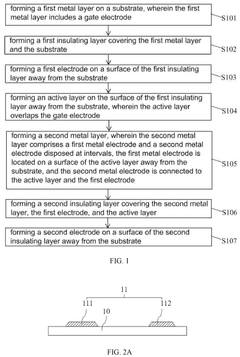
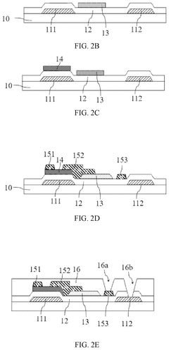
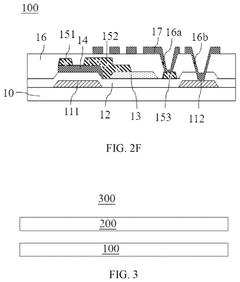
- The array substrate manufacturing method involves forming a first electrode on the surface of the insulating layer away from the substrate, with the active layer overlapping the gate, and a second metal layer comprising electrodes at intervals, allowing connection without via holes, thereby reducing the number of photomasks needed for forming via holes and overall photomasks required.
Material Sustainability and Environmental Impact Assessment
The environmental impact of IGZO (Indium Gallium Zinc Oxide) thin films in energy harvesting systems presents a complex sustainability profile that requires thorough assessment. IGZO materials offer significant advantages over conventional silicon-based semiconductors, including reduced material consumption due to their thin-film nature and lower processing temperatures, which translate to decreased energy requirements during manufacturing.
However, the sustainability concerns cannot be overlooked. Indium, a key component of IGZO, is classified as a critical raw material with limited global reserves. Current extraction rates and increasing demand for transparent conductive oxides in various applications raise serious questions about long-term availability. The mining processes associated with indium extraction also generate substantial environmental burdens, including habitat disruption, water pollution, and energy-intensive refinement procedures.
Life cycle assessment (LCA) studies comparing IGZO with alternative thin-film technologies reveal mixed results. While IGZO demonstrates lower energy payback times in energy harvesting applications compared to amorphous silicon, the end-of-life management remains problematic. The complex composition of IGZO makes recycling technically challenging and economically unfavorable under current recovery technologies.
Recent innovations in green manufacturing techniques for IGZO thin films show promise for reducing environmental impact. Solution-based processing methods using less toxic solvents and lower temperature deposition techniques have emerged as viable alternatives to conventional vacuum-based processes. These approaches not only reduce energy consumption but also minimize hazardous waste generation during production.
The integration of IGZO in energy harvesting systems creates an interesting sustainability paradox. While these systems generate clean energy during operation, potentially offsetting their embodied environmental costs, the initial material sourcing and manufacturing impacts remain significant. Research indicates that IGZO-based energy harvesters need to operate for 1-3 years (depending on application scenario) to achieve carbon neutrality when considering their full life cycle emissions.
Material substitution research represents a critical pathway toward enhanced sustainability. Efforts to develop indium-free alternatives using more abundant elements like aluminum, titanium, or tin oxide compounds are gaining momentum. Though these alternatives currently show lower performance metrics, their improved sustainability profiles may justify adoption in less demanding energy harvesting applications.
Regulatory frameworks worldwide are increasingly addressing the environmental implications of electronic materials like IGZO. Extended producer responsibility policies, restrictions on hazardous substances, and emerging circular economy directives will likely shape the future development and deployment of IGZO thin films in energy harvesting systems, driving further innovations in material sustainability.
Integration Challenges with Existing Energy Infrastructure
The integration of IGZO (Indium Gallium Zinc Oxide) thin film technology into existing energy infrastructure presents significant challenges that require careful consideration. Current energy systems are predominantly designed around conventional silicon-based technologies, creating compatibility issues when introducing IGZO-based energy harvesting solutions. These systems often lack the necessary interfaces and control mechanisms to efficiently incorporate and manage the unique electrical characteristics of IGZO thin films.
Physical integration constraints pose another major challenge. IGZO-based energy harvesting devices typically feature different form factors and mounting requirements compared to traditional energy components. Retrofitting these devices into existing infrastructure often requires substantial modifications to physical spaces, mounting systems, and protective enclosures, increasing implementation costs and complexity.
Electrical compatibility issues further complicate integration efforts. IGZO thin films generally produce DC power with variable voltage and current profiles that differ from conventional energy sources. This necessitates specialized power conditioning circuits, voltage regulators, and energy storage solutions to ensure seamless integration with AC-based grid systems or existing DC power networks.
Regulatory and standardization barriers also impede widespread adoption. Current energy codes and standards were developed without consideration for IGZO-based technologies, creating compliance challenges for system designers and installers. The lack of established certification pathways for these novel energy harvesting solutions often results in lengthy approval processes and additional testing requirements.
Maintenance and operational considerations present ongoing challenges after installation. Existing maintenance protocols and diagnostic tools are not designed to address the specific degradation mechanisms and failure modes of IGZO thin films. This knowledge gap necessitates specialized training for technical personnel and the development of new maintenance procedures tailored to these advanced materials.
Economic factors further complicate integration efforts. The cost-benefit analysis for incorporating IGZO-based energy harvesting systems must account for not only the technology itself but also the substantial modifications required to existing infrastructure. Without clear financial incentives or demonstrated long-term reliability, facility managers and energy system operators remain hesitant to invest in these emerging technologies.
Addressing these integration challenges requires a multidisciplinary approach involving materials scientists, electrical engineers, system integrators, and regulatory experts. Development of standardized interfaces, plug-and-play solutions, and comprehensive integration guidelines will be essential to facilitate broader adoption of IGZO thin film technology in energy harvesting applications across existing infrastructure.
Unlock deeper insights with Patsnap Eureka Quick Research — get a full tech report to explore trends and direct your research. Try now!
Generate Your Research Report Instantly with AI Agent
Supercharge your innovation with Patsnap Eureka AI Agent Platform!