IGZO Thin Film in Flexible Electronics Applications
SEP 28, 20259 MIN READ
Generate Your Research Report Instantly with AI Agent
Patsnap Eureka helps you evaluate technical feasibility & market potential.
IGZO Technology Evolution and Objectives
Indium Gallium Zinc Oxide (IGZO) thin film technology represents a significant advancement in semiconductor materials, emerging in the early 2000s as a promising alternative to amorphous silicon (a-Si) and low-temperature polysilicon (LTPS). The evolution of IGZO began with fundamental research at Tokyo Institute of Technology by Professor Hideo Hosono's team, who first demonstrated its unique properties as a transparent semiconductor in 2004. This breakthrough addressed critical limitations in existing thin-film transistor (TFT) technologies, particularly electron mobility and power consumption.
The technological trajectory of IGZO has been characterized by steady improvements in material composition, deposition techniques, and integration methods. Initially, IGZO films suffered from stability issues and inconsistent performance. However, refinements in sputtering processes and post-deposition treatments have significantly enhanced reliability, with electron mobility increasing from approximately 5-10 cm²/Vs in early implementations to 15-20 cm²/Vs in current advanced formulations.
A pivotal development occurred around 2012 when Sharp Corporation commercialized the first IGZO-based displays, demonstrating the technology's viability for mass production. This industrial adoption accelerated research into flexible applications, as IGZO's ability to maintain performance characteristics under mechanical stress became increasingly valuable for emerging form factors in electronics.
The primary technical objectives for IGZO thin films in flexible electronics applications center on several key parameters. First, achieving consistent electrical performance under mechanical deformation remains crucial, with targets for maintaining mobility above 10 cm²/Vs at bending radii below 5mm. Second, enhancing long-term stability under repeated flexing cycles presents a significant challenge, with industry targets exceeding 100,000 cycles without performance degradation.
Additional objectives include reducing the deposition temperature below 200°C to enable compatibility with a wider range of flexible substrates, particularly heat-sensitive polymers like polyethylene terephthalate (PET). Concurrently, researchers aim to improve the threshold voltage stability under bias stress conditions, which becomes particularly challenging in flexible implementations due to additional mechanical stresses.
The evolution trajectory points toward multi-component oxide semiconductors that build upon IGZO's foundation. These next-generation materials seek to further enhance electron mobility while maintaining the advantageous low-temperature processability and transparency. Recent research indicates potential for mobility values exceeding 30 cm²/Vs through careful control of oxygen vacancies and incorporation of additional elements such as hafnium or titanium.
Flexible Electronics Market Demand Analysis
The flexible electronics market has witnessed substantial growth over the past decade, driven primarily by increasing consumer demand for portable, lightweight, and durable electronic devices. Current market analysis indicates that the global flexible electronics market is projected to reach $42 billion by 2027, with a compound annual growth rate of approximately 11% from 2022 to 2027. Within this expanding market, IGZO (Indium Gallium Zinc Oxide) thin film technology has emerged as a critical component, particularly for display applications that require both flexibility and high performance.
Consumer electronics represents the largest application segment for flexible electronics incorporating IGZO thin films. Smartphones and tablets with flexible displays have gained significant market traction, with major manufacturers like Samsung, LG, and Apple investing heavily in this technology. Market research shows that consumer preference for devices with larger screens that remain portable has created strong demand for foldable and rollable displays where IGZO thin films offer superior electron mobility compared to traditional amorphous silicon.
Healthcare applications present another rapidly growing market segment for IGZO-based flexible electronics. Wearable health monitoring devices, including smart patches and electronic skin applications, are projected to grow at 15% annually through 2026. These devices benefit from IGZO's low power consumption and high transparency, enabling longer battery life and better integration with biological monitoring systems.
The automotive industry has also begun incorporating flexible displays utilizing IGZO technology in dashboard systems and entertainment consoles. Market forecasts suggest that by 2025, over 30% of premium vehicles will feature some form of flexible display technology, representing a significant new market opportunity for IGZO thin film applications.
Geographically, Asia-Pacific dominates the flexible electronics market, accounting for approximately 45% of global demand, with South Korea, Japan, and Taiwan leading in both production and consumption. North America and Europe follow with growing adoption rates in medical and industrial applications.
Supply chain analysis reveals increasing demand for indium, a key component in IGZO manufacturing, potentially creating material constraints as production scales. This has prompted research into alternative materials and more efficient deposition techniques to ensure sustainable market growth.
Market barriers include relatively high manufacturing costs compared to conventional display technologies and technical challenges in achieving consistent performance across large-area flexible substrates. However, as production scales and technology matures, analysts expect these barriers to diminish, further accelerating market adoption of IGZO-based flexible electronics across multiple industries.
IGZO Thin Film Development Status and Barriers
IGZO (Indium Gallium Zinc Oxide) thin film technology has emerged as a pivotal advancement in flexible electronics, offering superior electron mobility compared to conventional amorphous silicon. Currently, the global development of IGZO thin films demonstrates significant regional disparities, with East Asian countries—particularly Japan, South Korea, and Taiwan—leading in both research output and commercial applications. Japanese corporations like Sharp and semiconductor manufacturers in South Korea have established robust intellectual property portfolios in this domain.
The current technical maturity of IGZO thin films varies across applications. For display technologies, IGZO has achieved commercial viability, being incorporated into mass-produced flexible OLED and LCD displays. However, in more demanding applications such as flexible sensors and integrated circuits, the technology remains predominantly at the advanced research or early commercialization stages, requiring further refinement before widespread adoption.
A primary technical barrier facing IGZO thin film development is stability under mechanical stress. When subjected to repeated bending or folding, IGZO films often exhibit microcracks and performance degradation, limiting their durability in truly flexible applications. Research indicates that films below 20nm thickness show improved flexibility, but this comes at the cost of reduced electrical performance and increased susceptibility to environmental factors.
Environmental sensitivity presents another significant challenge. IGZO thin films demonstrate performance variations under different humidity and temperature conditions, with electron mobility decreasing notably in high-humidity environments. This necessitates effective encapsulation technologies, which themselves must maintain flexibility while providing hermetic protection—a complex engineering challenge that has not been fully resolved.
Manufacturing scalability remains problematic for high-performance IGZO applications. While sputtering techniques are well-established for display production, achieving the uniformity and precision required for advanced flexible electronics across large substrates presents considerable difficulties. Variations in film thickness and composition can lead to inconsistent device performance, particularly problematic for applications requiring tight parameter control.
Interface engineering between IGZO and adjacent layers in device structures represents another technical hurdle. Contact resistance at metal-IGZO interfaces and charge trapping at dielectric-IGZO boundaries can significantly impair device performance. Recent research has focused on interface modification techniques and novel dielectric materials, but optimal solutions balancing performance, flexibility, and manufacturing feasibility remain elusive.
The cost structure of high-quality IGZO production also presents barriers to widespread adoption. Indium, a key component, faces supply constraints and price volatility due to limited global reserves. Alternative compositions with reduced indium content are under investigation but currently demonstrate inferior performance characteristics compared to standard IGZO formulations.
Current IGZO Implementation in Flexible Devices
01 IGZO thin film transistor fabrication methods
Various methods for fabricating IGZO (Indium Gallium Zinc Oxide) thin film transistors with improved performance characteristics. These methods include specific deposition techniques, annealing processes, and structural optimizations to enhance carrier mobility, stability, and electrical properties. The fabrication processes often involve controlling oxygen content, layer thickness, and interface quality to achieve desired semiconductor properties.- IGZO thin film fabrication methods: Various methods for fabricating IGZO (Indium Gallium Zinc Oxide) thin films, including sputtering, chemical vapor deposition, and solution processing techniques. These methods focus on controlling the deposition parameters to achieve desired film properties such as thickness uniformity, crystallinity, and electrical characteristics. The fabrication processes often involve specific temperature treatments and atmospheric conditions to optimize the semiconductor performance.
- IGZO thin film transistor (TFT) structures: Design and architecture of thin film transistors using IGZO as the semiconductor layer. These structures include various configurations such as bottom-gate, top-gate, dual-gate, and vertical architectures. The designs focus on optimizing channel dimensions, gate dielectric materials, and electrode configurations to enhance transistor performance metrics including mobility, on/off ratio, threshold voltage stability, and subthreshold swing.
- IGZO composition and doping strategies: Modification of IGZO thin film composition through doping and stoichiometry control to enhance electrical properties. Various dopants and compositional ratios of indium, gallium, and zinc are explored to optimize carrier concentration, mobility, and stability. Techniques include incorporation of elements such as hafnium, titanium, or aluminum to modify the band structure and improve device performance under different operating conditions.
- IGZO thin film stability and passivation: Methods to improve the environmental and operational stability of IGZO thin films through passivation layers and surface treatments. These approaches address issues such as bias stress instability, light sensitivity, and degradation under humid conditions. Passivation techniques include application of inorganic barrier layers, organic encapsulants, and interface engineering to reduce defect states and prevent atmospheric contamination.
- IGZO thin film applications in display and sensor technologies: Implementation of IGZO thin films in various electronic applications including display backplanes, touch sensors, and imaging devices. The high mobility and transparency of IGZO make it suitable for high-resolution displays, flexible electronics, and large-area sensor arrays. These applications leverage the unique combination of optical transparency, low processing temperature, and superior electrical characteristics of IGZO compared to conventional amorphous silicon technology.
02 IGZO thin film composition and doping strategies
Innovations in IGZO material composition and doping approaches to enhance thin film performance. These include adjusting the ratio of indium, gallium, and zinc, incorporating additional elements as dopants, and developing novel compound structures. Modified compositions aim to improve electron mobility, reduce defects, enhance stability against environmental factors, and optimize optical and electrical properties for specific applications.Expand Specific Solutions03 IGZO thin film display applications
Implementation of IGZO thin films in display technologies, including LCD and OLED panels. IGZO's high electron mobility and transparency make it ideal for display backplanes, enabling higher resolution, faster refresh rates, and lower power consumption. These applications leverage IGZO's ability to maintain electrical characteristics while being optically transparent, allowing for improved display performance and new form factors.Expand Specific Solutions04 IGZO thin film stability and passivation techniques
Methods to improve the stability and reliability of IGZO thin films through passivation and protective layers. These techniques address issues such as bias stress instability, environmental degradation, and threshold voltage shifts. Approaches include surface treatments, encapsulation layers, interface engineering, and thermal processing to reduce defects and trap states that affect long-term performance and reliability.Expand Specific Solutions05 IGZO thin film for flexible and next-generation electronics
Application of IGZO thin films in flexible, transparent, and next-generation electronic devices. The low-temperature processing capability of IGZO makes it suitable for deposition on flexible substrates, enabling bendable displays and wearable electronics. These applications exploit IGZO's unique combination of high performance at low processing temperatures, transparency, and mechanical flexibility for emerging technology platforms.Expand Specific Solutions
Leading IGZO and Flexible Electronics Manufacturers
The IGZO thin film technology in flexible electronics is currently in a growth phase, with the market expanding rapidly due to increasing demand for bendable displays and wearable devices. Major players like Samsung Display, LG Display, and BOE Technology are leading innovation, leveraging IGZO's advantages of high electron mobility, transparency, and low power consumption. Sharp Corp, which pioneered commercial IGZO displays, continues to hold significant technological expertise, while companies like E Ink are exploring IGZO for e-paper applications. The technology has reached moderate maturity in conventional displays but remains in early development stages for advanced flexible applications, with companies like Canon and Intermolecular focusing on improving manufacturing processes and material properties to enhance performance and reduce costs.
SAMSUNG DISPLAY CO LTD
Technical Solution: 三星显示在IGZO柔性电子领域采用了创新的技术路线,开发了"IGZO-LTPS混合背板"技术。该方案在柔性显示器的不同区域分别使用IGZO和LTPS技术,优化了性能与功耗平衡。三星的IGZO薄膜采用独特的四元组分配比(In:Ga:Zn:O=1:1:1:4),通过精确控制氧空位浓度,实现了高电子迁移率(>15 cm²/Vs)和低阈值电压漂移(<0.5V/1000h)[5]。制造工艺方面,三星开发了专有的原子层沉积(ALD)技术,在柔性基板上实现了高均匀性IGZO薄膜,厚度控制精度达±2nm。为解决柔性应用中的应力问题,三星设计了多层缓冲结构和应力释放图案,使IGZO薄膜在反复弯曲(半径<3mm)时保持稳定性能。该技术还采用了创新的封装方案,使用超薄无机/有机交替层(厚度<10μm)保护IGZO薄膜免受水氧侵蚀,延长了柔性设备寿命[6]。三星的IGZO技术已应用于其折叠屏手机和可穿戴设备中。
优势:混合背板技术充分发挥IGZO低功耗和LTPS高性能的优点;ALD工艺保证了薄膜高均匀性;应力释放设计提高了弯折耐久性;封装技术先进,水氧阻隔性能好。劣势:制造工艺复杂度高,设备投资大;混合背板增加了制造步骤和成本;在极端环境条件下可能存在可靠性挑战;技术整合难度大。
BOE Technology Group Co., Ltd.
Technical Solution: 京东方(BOE)在IGZO柔性电子领域开发了全面的技术方案,专注于大规模生产可行性。其核心是"氧化物半导体柔性背板"技术,采用优化的IGZO材料配比(In:Ga:Zn=2:2:1)和独特的多靶共溅射工艺,实现了均匀性>92%的大面积IGZO薄膜沉积。BOE的技术方案特别关注柔性基板与IGZO薄膜的界面工程,开发了专有的界面修饰层,提高了薄膜附着力和应力耐受性。其制造工艺采用低温(150-180°C)处理,兼容聚酰亚胺等柔性基板材料[7]。为解决柔性应用中的可靠性问题,BOE设计了创新的"岛状-桥接"结构,将刚性功能区域与柔性互连区域分离,使IGZO器件在弯曲状态下保持稳定性能,弯曲半径可达2.5mm,弯折寿命超过20万次。BOE还开发了专用的阻障封装技术,水汽透过率低于10^-6 g/m²/day,有效保护了IGZO薄膜免受环境影响[8]。该技术已成功应用于BOE的柔性AMOLED显示器和可折叠智能设备中,并扩展到柔性传感器和电子皮肤等新兴应用领域。
优势:大规模生产能力强,良率控制技术成熟;岛状-桥接结构提高了弯折可靠性;界面工程技术先进,薄膜附着力好;产品线丰富,应用场景广泛。劣势:IGZO性能与日韩企业相比仍有差距;极端弯折条件下可靠性有待提高;高端柔性显示技术仍依赖部分进口设备和材料;在高分辨率应用中电子迁移率限制性能。
Key IGZO Thin Film Patents and Technical Innovations
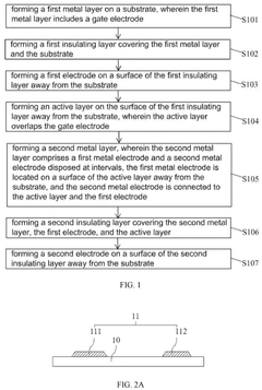
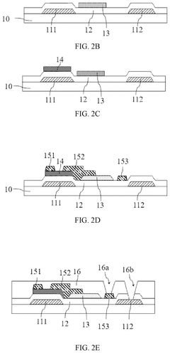
Array substrate and manufacturing method thereof, and display panel
PatentPendingUS20240355840A1
Innovation
- The array substrate manufacturing method involves forming a first electrode on the surface of the insulating layer away from the substrate, with the active layer overlapping the gate, and a second metal layer comprising electrodes at intervals, allowing connection without via holes, thereby reducing the number of photomasks needed for forming via holes and overall photomasks required.
Manufacturing Process Optimization for IGZO Films
The optimization of manufacturing processes for IGZO (Indium Gallium Zinc Oxide) films represents a critical challenge in advancing flexible electronics applications. Current manufacturing techniques primarily involve physical vapor deposition methods, with RF magnetron sputtering emerging as the industry standard due to its ability to produce high-quality films with consistent stoichiometry. However, significant process variables including substrate temperature, oxygen partial pressure, and post-deposition annealing conditions substantially impact the electrical and structural properties of IGZO films.
Recent advancements have focused on reducing deposition temperatures to enable compatibility with flexible polymer substrates. Traditional processes requiring temperatures above 300°C have been modified through innovative approaches such as high-pressure sputtering and plasma-enhanced deposition, allowing quality film formation at temperatures below 150°C. These low-temperature processes have demonstrated transistor mobility values approaching 10 cm²/Vs, which represents a significant achievement for flexible device applications.
The control of oxygen vacancies during film formation presents another critical manufacturing challenge. These vacancies function as electron donors and significantly influence carrier concentration and device stability. Advanced process monitoring techniques including in-situ optical emission spectroscopy and real-time resistivity measurements have been implemented to provide precise control over oxygen incorporation during deposition.
Post-deposition treatments have emerged as essential optimization steps. Techniques such as vacuum annealing, atmospheric pressure annealing, and photonic curing have shown promise in enhancing film crystallinity while maintaining compatibility with temperature-sensitive substrates. Particularly noteworthy is the development of pulsed laser annealing methods that enable localized heating of the IGZO layer without damaging underlying polymer substrates.
Roll-to-roll (R2R) processing represents the frontier of manufacturing optimization for flexible IGZO electronics. This continuous production approach offers significant throughput advantages compared to batch processing methods. Recent pilot-scale demonstrations have achieved web speeds of 5-10 meters per minute while maintaining transistor performance metrics comparable to those produced via conventional methods. Key challenges in R2R implementation include maintaining uniform tension and precise alignment during multi-layer deposition.
Thickness uniformity across large-area substrates remains problematic, with typical variations of ±5% observed in production environments. Advanced deposition systems incorporating multiple magnetron sources with optimized scanning patterns have demonstrated improvements, reducing thickness variations to below ±2% across 1-meter width substrates. This enhanced uniformity directly translates to improved device-to-device consistency in final products.
Sustainability Aspects of IGZO Flexible Electronics
The sustainability profile of IGZO (Indium Gallium Zinc Oxide) technology in flexible electronics represents a critical consideration for its long-term viability and environmental impact. IGZO offers several inherent sustainability advantages compared to conventional semiconductor materials, particularly in terms of energy efficiency. The low power consumption of IGZO-based devices—requiring approximately 80-90% less energy than traditional amorphous silicon alternatives—translates to extended battery life and reduced carbon footprint across product lifecycles.
Material composition presents both opportunities and challenges for IGZO sustainability. Indium, a key component, faces supply constraints as a relatively rare element primarily obtained as a byproduct of zinc mining. Current global reserves are estimated at approximately 15,000 tons, raising concerns about long-term availability for mass-market applications. This scarcity has prompted research into indium recycling technologies and alternative material compositions with reduced indium content.
Manufacturing processes for IGZO thin films have evolved toward greater sustainability through lower temperature deposition techniques. Modern sputtering and solution-processing methods can operate at temperatures below 200°C, enabling compatibility with recyclable polymer substrates and reducing energy requirements compared to traditional semiconductor fabrication. Additionally, the simplified transistor architecture of IGZO devices typically requires fewer manufacturing steps and chemical inputs.
End-of-life considerations represent an emerging focus area for IGZO flexible electronics. The integration of IGZO with biodegradable substrates has demonstrated promising results in laboratory settings, potentially enabling partially biodegradable electronic components. Research at Stanford University and the University of Tokyo has shown that certain IGZO formulations can be designed for controlled degradation in specific environmental conditions, though commercial implementation remains limited.
Lifecycle assessment studies indicate that IGZO flexible electronics can achieve a 30-40% reduction in overall environmental impact compared to rigid silicon-based alternatives when accounting for raw material extraction, manufacturing, use phase, and disposal. However, challenges remain in establishing effective recycling infrastructure for composite flexible electronics that incorporate multiple material types including IGZO layers.
Industry initiatives are increasingly addressing these sustainability challenges through collaborative approaches. The Sustainable Electronics Manufacturing Consortium has established guidelines for IGZO manufacturing that emphasize reduced solvent use, energy-efficient deposition, and design for disassembly principles to facilitate eventual recycling of valuable materials.
Unlock deeper insights with Patsnap Eureka Quick Research — get a full tech report to explore trends and direct your research. Try now!
Generate Your Research Report Instantly with AI Agent
Supercharge your innovation with Patsnap Eureka AI Agent Platform!