IGZO Thin Film and its Compliance with Global Display Regulations
SEP 28, 202510 MIN READ
Generate Your Research Report Instantly with AI Agent
Patsnap Eureka helps you evaluate technical feasibility & market potential.
IGZO Technology Background and Development Goals
Indium Gallium Zinc Oxide (IGZO) thin film technology represents a significant advancement in semiconductor materials for display applications. First developed in the early 2000s by researchers at Tokyo Institute of Technology, IGZO emerged as a promising alternative to amorphous silicon (a-Si) and low-temperature polysilicon (LTPS) for thin-film transistors (TFTs). The fundamental innovation of IGZO lies in its unique electronic structure, which combines the stability of amorphous materials with the high electron mobility typically associated with crystalline semiconductors.
The evolution of IGZO technology has been driven by increasing demands for higher resolution, lower power consumption, and enhanced performance in display technologies. Traditional a-Si TFTs faced limitations in electron mobility (typically 0.5-1 cm²/Vs), while IGZO demonstrated capabilities of 10-20 cm²/Vs, enabling faster switching speeds and higher pixel densities. This breakthrough addressed critical bottlenecks in the development of high-resolution displays for mobile devices, tablets, and large-format screens.
From 2010 to 2020, IGZO technology matured significantly, with major display manufacturers including Sharp, LG Display, and Samsung incorporating IGZO TFTs into commercial products. The technology's trajectory has been characterized by continuous improvements in deposition techniques, material composition, and integration with existing manufacturing processes. Particularly noteworthy has been the development of oxide semiconductor variations that optimize specific performance parameters for different display applications.
The primary technical goals for IGZO thin film development currently focus on several key areas. First, enhancing stability under various environmental conditions, particularly addressing threshold voltage shifts under prolonged bias stress and illumination. Second, improving uniformity across large substrates to enable cost-effective production of larger displays. Third, reducing manufacturing costs through optimized deposition processes and integration with existing fabrication lines.
Regulatory compliance has emerged as a critical consideration in IGZO development. As global display regulations become increasingly stringent regarding energy efficiency, hazardous materials, and end-of-life recycling, IGZO technology must evolve to meet these requirements. The European Union's Restriction of Hazardous Substances (RoHS) directive, Energy-related Products (ErP) directive, and similar regulations in North America and Asia have established frameworks that directly impact material selection and manufacturing processes for display technologies.
Looking forward, IGZO technology aims to expand beyond traditional display applications into emerging fields such as flexible electronics, transparent displays, and sensor arrays. The development roadmap includes achieving electron mobility exceeding 50 cm²/Vs, further reducing power consumption by optimizing off-state current characteristics, and enhancing compatibility with next-generation display technologies such as microLED and quantum dot displays.
Market Demand Analysis for IGZO Display Technology
The global display market has witnessed a significant shift towards advanced display technologies, with IGZO (Indium Gallium Zinc Oxide) thin film transistors emerging as a pivotal innovation. Market analysis indicates that the demand for IGZO display technology is primarily driven by the growing consumer preference for high-resolution, energy-efficient displays across multiple device categories.
Consumer electronics represent the largest market segment for IGZO technology, with smartphones and tablets leading adoption. The global smartphone market, valued at approximately 500 billion USD, increasingly demands displays with higher refresh rates and lower power consumption—attributes where IGZO excels. Market research shows that premium smartphone manufacturers have begun incorporating IGZO displays to differentiate their products, with adoption rates growing at 15% annually since 2019.
Television and monitor segments present substantial growth opportunities for IGZO technology. The premium TV market segment has shown particular interest in IGZO backplanes for OLED and advanced LCD displays, as consumers seek thinner, more energy-efficient large-screen options. Market forecasts predict that IGZO-based displays will capture 25% of the premium TV market by 2025, representing a significant expansion from current levels.
The automotive display sector represents an emerging high-value market for IGZO technology. As vehicles incorporate more sophisticated infotainment systems and digital dashboards, the demand for displays that perform reliably across extreme temperature ranges while consuming minimal power has intensified. Industry analysts project the automotive display market to grow at 22% CAGR through 2027, with IGZO-based solutions positioned to capture a substantial portion of this growth.
Healthcare and industrial applications constitute specialized but lucrative market segments for IGZO display technology. Medical imaging devices require exceptional clarity and reliability, while industrial control systems often operate in challenging environments—both scenarios where IGZO's performance characteristics provide meaningful advantages. These sectors, though smaller in volume, offer higher margins and more stable demand patterns.
Regional analysis reveals that East Asia dominates IGZO display manufacturing, with Japan, South Korea, and Taiwan accounting for over 80% of production capacity. However, consumption patterns show more geographic diversity, with North America and Europe representing significant markets for premium devices incorporating IGZO technology.
Market barriers include the higher initial manufacturing costs compared to conventional a-Si TFT technology and the technical complexity of IGZO fabrication processes. However, as production scales and manufacturing processes mature, these cost differentials are expected to narrow, accelerating market penetration across more price-sensitive segments.
IGZO Thin Film Technical Challenges and Global Status
IGZO (Indium Gallium Zinc Oxide) thin film technology has emerged as a revolutionary material in the display industry, offering significant advantages over traditional amorphous silicon (a-Si) technology. Globally, the development and implementation of IGZO technology faces varying regulatory landscapes that impact its adoption and commercialization. Current technical challenges primarily revolve around material stability, manufacturing scalability, and compliance with increasingly stringent environmental regulations.
The technical status of IGZO thin film technology varies significantly across regions. Japan leads in IGZO research and development, with companies like Sharp Corporation pioneering commercial applications. South Korea follows closely with Samsung and LG making substantial investments in IGZO technology integration. Taiwan has established itself as a manufacturing hub for IGZO panels, while mainland China is rapidly expanding its capabilities through government-backed initiatives and investments in display technology.
In Europe, IGZO adoption faces more rigorous environmental and health regulations, particularly concerning indium usage, which is classified as a critical raw material with supply constraints. The European Union's Restriction of Hazardous Substances (RoHS) and Registration, Evaluation, Authorization and Restriction of Chemicals (REACH) regulations impose strict guidelines on material composition and manufacturing processes.
The United States market presents a different regulatory environment, focusing more on performance standards and intellectual property protection rather than material restrictions. This has allowed for innovative applications of IGZO technology in specialized sectors such as military displays and medical imaging devices.
Key technical challenges currently limiting IGZO's global expansion include threshold voltage instability under prolonged bias stress, particularly in high-temperature environments. This instability affects display reliability and longevity, requiring additional compensation circuits that increase production costs. Manufacturing yield rates remain inconsistent at larger scales, with defect densities increasing proportionally with panel size.
Environmental concerns represent another significant challenge, as indium extraction and processing have substantial ecological impacts. The limited global supply of indium raises sustainability questions about IGZO's long-term viability as display sizes increase and applications diversify. Additionally, end-of-life recycling processes for IGZO panels are still underdeveloped, creating potential conflicts with circular economy regulations being implemented in various regions.
Radiation hardness and reliability in extreme environments remain challenges for specialized applications in aerospace and automotive industries, where temperature fluctuations and exposure to radiation can significantly impact IGZO performance characteristics. These technical limitations must be addressed to meet the stringent reliability requirements of these high-value sectors.
Current IGZO Thin Film Implementation Solutions
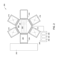
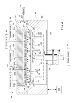
01 IGZO thin film fabrication methods
Various methods for fabricating Indium Gallium Zinc Oxide (IGZO) thin films, including sputtering, chemical vapor deposition, and solution processing techniques. These methods focus on controlling the deposition parameters to achieve optimal film quality, uniformity, and electrical properties. The fabrication processes often involve specific temperature conditions, gas environments, and post-deposition treatments to enhance the performance of the IGZO thin films.- IGZO thin film fabrication methods: Various methods for fabricating Indium Gallium Zinc Oxide (IGZO) thin films, including sputtering, chemical vapor deposition, and solution processing techniques. These methods control the crystallinity, composition, and thickness of the IGZO layer to achieve desired electrical properties. Process parameters such as temperature, pressure, and gas flow rates significantly impact the quality and performance of the resulting thin films.
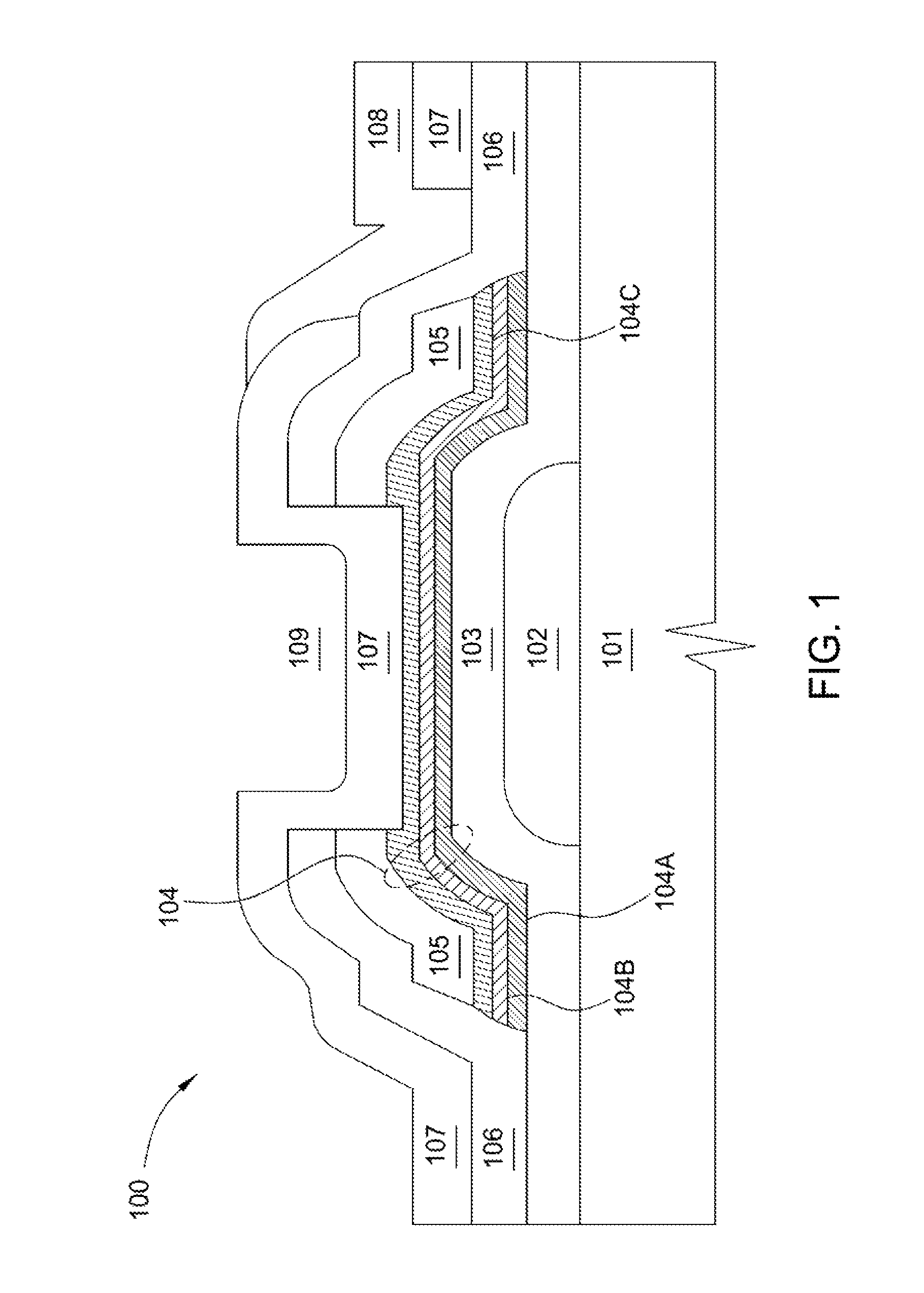
- IGZO thin film transistor (TFT) structures: Different structural configurations of IGZO-based thin film transistors, including bottom-gate, top-gate, and dual-gate architectures. These structures incorporate various electrode materials, dielectric layers, and channel designs to optimize device performance. The transistor structures are designed to enhance mobility, stability, and reliability while minimizing leakage current and threshold voltage shift.
- IGZO thin film composition and doping: Modifications to the composition of IGZO thin films through doping and stoichiometric adjustments to enhance electrical properties. Various dopants including metals and non-metals are incorporated to control carrier concentration, mobility, and stability. The ratio of indium, gallium, and zinc significantly affects the semiconductor characteristics, with higher indium content generally resulting in higher mobility while gallium helps stabilize the amorphous phase.
- IGZO thin film applications in display technology: Implementation of IGZO thin films in various display technologies including LCD, OLED, and flexible displays. IGZO's high electron mobility and transparency make it ideal for high-resolution, energy-efficient displays. These thin films enable faster refresh rates, higher pixel densities, and lower power consumption compared to conventional amorphous silicon technology, while also supporting the development of transparent and flexible display panels.
- IGZO thin film post-treatment and stability enhancement: Post-deposition treatments and passivation techniques to improve the stability and reliability of IGZO thin films. These include thermal annealing, plasma treatment, and passivation layer deposition to reduce defects, control oxygen vacancies, and enhance environmental stability. Various encapsulation methods are employed to protect IGZO films from moisture and oxygen, which can degrade performance over time. These treatments significantly improve device lifetime and operational stability under various environmental conditions.
02 IGZO thin film transistor structures
Different structural designs of thin film transistors (TFTs) using IGZO as the semiconductor layer. These structures include bottom-gate, top-gate, dual-gate, and vertical configurations, each offering specific advantages in terms of performance, stability, and manufacturing complexity. The designs often incorporate various buffer layers, passivation materials, and electrode configurations to optimize the electrical characteristics and reliability of the IGZO TFTs.Expand Specific Solutions03 IGZO composition and doping strategies
Optimization of IGZO material composition and doping approaches to enhance specific properties of the thin films. This includes adjusting the In:Ga:Zn ratio, incorporating additional elements such as hafnium, titanium, or silicon, and controlling oxygen vacancies. These compositional modifications aim to improve carrier mobility, threshold voltage stability, and resistance to environmental degradation, making the IGZO thin films more suitable for various electronic applications.Expand Specific Solutions04 IGZO thin film applications in display technology
Implementation of IGZO thin films in various display technologies, including LCD, OLED, and flexible displays. IGZO's high electron mobility, low off-current, and transparency make it particularly suitable for backplane circuits in high-resolution and energy-efficient displays. The applications extend to touch panels, transparent displays, and large-area display panels where uniform electrical characteristics across the substrate are crucial.Expand Specific Solutions05 IGZO thin film reliability and stability enhancement
Methods to improve the reliability and stability of IGZO thin films under various operational and environmental conditions. These include passivation techniques, annealing processes, and interface engineering to reduce threshold voltage shifts, hysteresis, and degradation under bias stress. The approaches focus on mitigating the effects of oxygen vacancies, water absorption, and charge trapping at interfaces, which are common causes of instability in IGZO-based devices.Expand Specific Solutions
Key Industry Players in IGZO Display Manufacturing
The IGZO thin film display technology market is currently in a growth phase, with increasing adoption across various display applications due to its superior electron mobility and power efficiency. The global market size is expanding rapidly, driven by demand for high-resolution, energy-efficient displays in consumer electronics and commercial applications. From a technical maturity perspective, major players like Samsung Display, LG Display, and Sharp Corp. have achieved commercial-scale production, with Sharp being the pioneer in IGZO technology. Asian manufacturers dominate the landscape, with BOE Technology, TCL China Star Optoelectronics, and Japan-based companies like ULVAC and Toppan Holdings providing critical manufacturing equipment and materials. Regulatory compliance remains a key focus as these companies navigate different regional standards while expanding their global market presence.
BOE Technology Group Co., Ltd.
Technical Solution: BOE Technology has developed a comprehensive IGZO thin film technology platform as part of their advanced display portfolio. Their approach focuses on optimizing the composition and deposition parameters of IGZO layers to achieve high electron mobility while maintaining manufacturing scalability. BOE's implementation features a proprietary multi-layer structure that enhances stability and performance of the oxide semiconductor. Their IGZO displays incorporate specialized barrier and passivation layers that protect the sensitive semiconductor material from environmental factors and extend operational lifespan. BOE has established rigorous compliance protocols for their IGZO technology, ensuring adherence to global regulations including RoHS, REACH, and various regional environmental standards. Their manufacturing process includes advanced material purification techniques that minimize the presence of restricted substances while maintaining performance characteristics. BOE's IGZO panels typically achieve 40-60% power reduction compared to conventional a-Si displays while supporting higher refresh rates and resolution, making them compliant with energy efficiency standards worldwide. The company has scaled their IGZO technology across multiple production lines, enabling application in diverse products from smartphones to large-format professional displays.
Strengths: Massive production capacity allowing for economies of scale, strong vertical integration from materials to finished displays, and competitive pricing structure. BOE's IGZO technology demonstrates good uniformity across large panel sizes. Weaknesses: Slightly lower electron mobility compared to Japanese competitors, challenges with ultra-high resolution implementations, and occasional yield issues with new generation products.
SAMSUNG DISPLAY CO LTD
Technical Solution: Samsung Display has developed advanced IGZO thin film technology as part of their oxide TFT portfolio, though they primarily market it under their proprietary oxide semiconductor branding. Their approach combines IGZO with their metal oxide TFT technology to create high-performance, energy-efficient displays that comply with global regulations. Samsung's implementation features a unique multi-layer deposition process that enhances electron mobility while reducing impurities in the semiconductor layer. Their manufacturing protocol includes rigorous testing for hazardous substances to ensure compliance with RoHS, REACH, and other international standards. Samsung has optimized their IGZO-based displays for ultra-high resolution applications, achieving pixel densities exceeding 500 PPI while maintaining power efficiency. Their technology incorporates specialized passivation layers that protect the oxide semiconductor from environmental degradation, extending display lifespan and stability. Samsung's displays typically feature reduced bezel sizes due to the smaller TFT size possible with IGZO technology, while their advanced compensation circuits minimize image sticking issues common in some oxide semiconductor implementations.
Strengths: Exceptional production scale capabilities, vertical integration from materials to finished displays, and strong optimization for mobile device applications with industry-leading resolution and brightness. Weaknesses: Higher manufacturing complexity requiring specialized equipment, challenges with yield rates for larger panels, and relatively higher cost structure compared to conventional a-Si technology.
Critical Patents and Technical Innovations in IGZO
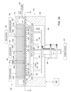
Apparatus and method of forming an indium gallium zinc oxide layer
PatentActiveUS9214340B2
Innovation
- A method and apparatus for forming a multi-element containing film using a gas distribution plate assembly with a precursor plenum and heat exchanging channel, allowing for precise control of precursor gas flow and composition, enabling the deposition of IGZO layers with tailored stoichiometry and reduced environmental exposure.
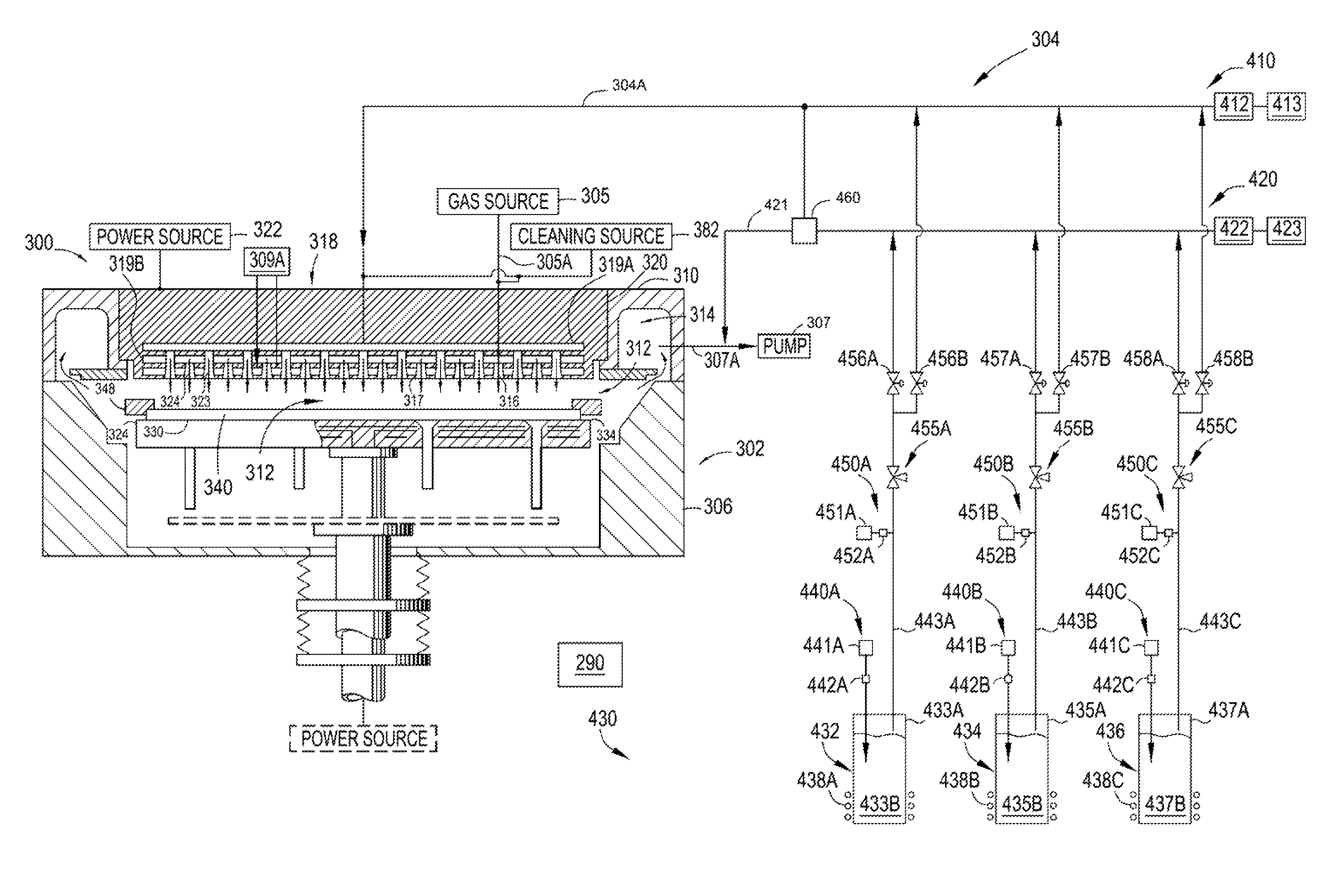

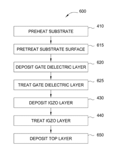
Indium gallium zinc oxide layers for thin film transistors
PatentInactiveUS9502242B2
Innovation
- The use of chemical vapor deposition (CVD) processes for forming IGZO active layers without a prior nucleation layer, combined with in-situ substrate cleaning and preheating, allows for the deposition of high-mobility IGZO layers with controlled stoichiometry and reduced exposure to air, improving throughput and reducing environmental degradation.

Global Regulatory Compliance Framework for Display Technologies
The global regulatory landscape for display technologies has become increasingly complex as environmental and health concerns drive stricter standards worldwide. IGZO (Indium Gallium Zinc Oxide) thin film technology must navigate this intricate framework of regulations that varies significantly across regions. Understanding these compliance requirements is essential for manufacturers and developers integrating IGZO technology into display products.
In the European Union, the Restriction of Hazardous Substances (RoHS) Directive and Registration, Evaluation, Authorization and Restriction of Chemicals (REACH) regulations directly impact IGZO thin film manufacturing. These frameworks limit the use of hazardous materials such as heavy metals and require thorough documentation of chemical substances used in production processes. The EU's Ecodesign Directive further mandates energy efficiency standards that IGZO displays must meet.
North American regulations present a different compliance landscape. The United States Environmental Protection Agency (EPA) enforces the Toxic Substances Control Act (TSCA), which requires reporting and testing of chemical substances. California's Proposition 65 imposes additional labeling requirements for products containing substances known to cause cancer or reproductive harm. IGZO manufacturers must ensure their thin film production processes and final products comply with these state-specific regulations.
In Asia, Japan's Chemical Substances Control Law (CSCL) and China's Restriction of Hazardous Substances (China RoHS) create another layer of compliance requirements. South Korea's Act on Resource Circulation of Electrical and Electronic Equipment and Vehicles imposes strict recycling and material composition standards. These Asian regulations are particularly relevant as many IGZO display manufacturing facilities are located in this region.
Energy efficiency certifications represent another critical compliance area. ENERGY STAR in the United States, TCO Certification in Europe, and various national energy efficiency standards establish power consumption limits that directly influence IGZO thin film design parameters. The technology's inherent low power consumption characteristics provide advantages in meeting these requirements.
End-of-life considerations are increasingly important in global regulations. The EU's Waste Electrical and Electronic Equipment (WEEE) Directive and similar legislation in other regions mandate recyclability and proper disposal of display components. IGZO thin film composition must be designed with these requirements in mind, ensuring materials can be properly recovered or safely disposed of at product end-of-life.
Emerging regulations around nanomaterials may also impact IGZO technology as regulatory bodies develop frameworks to address potential health and environmental concerns related to engineered nanoscale materials. Manufacturers must monitor these developing regulations closely as they may introduce new compliance requirements for thin film technologies.
Environmental Impact and Sustainability of IGZO Manufacturing
The manufacturing processes of IGZO (Indium Gallium Zinc Oxide) thin films present significant environmental considerations that must be addressed as the technology continues to expand in the display industry. Traditional semiconductor manufacturing has historically involved hazardous chemicals, high energy consumption, and substantial waste generation. IGZO production, while more efficient than some alternatives, still faces similar sustainability challenges.
Primary environmental concerns include the extraction and processing of rare metals, particularly indium, which is classified as a critical raw material due to supply risks and economic importance. Current mining practices for these materials often result in habitat destruction, water pollution, and high carbon emissions. The semiconductor fabrication process itself requires substantial energy inputs, ultra-pure water resources, and specialized gases that contribute to greenhouse emissions.
Recent advancements in IGZO manufacturing have focused on reducing environmental impact through improved deposition techniques. Compared to conventional amorphous silicon (a-Si) processes, IGZO fabrication can be conducted at lower temperatures, resulting in approximately 30-40% energy savings. Additionally, the extended lifetime and higher efficiency of IGZO-based displays contribute to reduced electronic waste generation over product lifecycles.
Several leading manufacturers have implemented closed-loop water systems that recycle up to 90% of water used in production facilities. Waste reduction initiatives have also shown promise, with some facilities reporting 15-20% decreases in hazardous waste generation through process optimization and material recovery systems. These improvements align with increasingly stringent global environmental regulations, including the EU's Restriction of Hazardous Substances (RoHS) directive and various national electronic waste management policies.
Life cycle assessments of IGZO-based displays indicate potential for reduced environmental footprint compared to conventional technologies. The extended lifespan, lower power consumption, and reduced material requirements contribute to sustainability advantages when evaluated across the entire product lifecycle. However, end-of-life considerations remain challenging, as the recovery of rare metals from disposed displays continues to present technical and economic barriers.
Industry consortiums and research institutions are actively developing more sustainable manufacturing approaches, including alternative precursor materials, solvent-free deposition methods, and improved recycling technologies. These initiatives aim to address the full environmental impact of IGZO technology while maintaining its performance advantages in display applications. The development of these sustainable practices will be crucial for ensuring IGZO compliance with increasingly stringent global environmental regulations while meeting market demands for greener electronics.
Unlock deeper insights with Patsnap Eureka Quick Research — get a full tech report to explore trends and direct your research. Try now!
Generate Your Research Report Instantly with AI Agent
Supercharge your innovation with Patsnap Eureka AI Agent Platform!