IGZO Thin Film: A Study of its Integration with Organic Electronics
SEP 28, 20259 MIN READ
Generate Your Research Report Instantly with AI Agent
Patsnap Eureka helps you evaluate technical feasibility & market potential.
IGZO Thin Film Technology Evolution and Objectives
Indium Gallium Zinc Oxide (IGZO) thin film technology represents a significant advancement in semiconductor materials, emerging as a promising alternative to conventional amorphous silicon (a-Si) and polycrystalline silicon (poly-Si) in the field of thin-film transistors (TFTs). First developed in the early 2000s by researchers at Tokyo Institute of Technology, IGZO has evolved from a laboratory curiosity to a commercially viable technology over the past two decades.
The evolution of IGZO thin film technology can be traced through several key developmental phases. Initially, research focused on understanding the fundamental properties of this oxide semiconductor, particularly its unique electron transport mechanisms and stability characteristics. By 2010, significant progress had been made in optimizing deposition techniques, primarily through radio frequency (RF) sputtering and pulsed laser deposition (PLD) methods, enabling the creation of uniform IGZO films with controlled stoichiometry.
A critical milestone was reached in 2012 when Sharp Corporation introduced the first commercial display products incorporating IGZO technology, demonstrating superior performance in terms of power efficiency and resolution compared to traditional a-Si TFT displays. This commercial breakthrough accelerated research interest and industrial investment in IGZO technology globally.
The integration of IGZO with organic electronics represents a particularly promising frontier in this technological evolution. Unlike conventional silicon-based semiconductors, IGZO offers compatibility with flexible substrates and low-temperature processing, making it highly suitable for integration with organic electronic components. This compatibility stems from IGZO's ability to maintain stable electrical characteristics even when deposited at relatively low temperatures (below 300°C), aligning well with the thermal constraints of organic materials.
Current technological objectives in IGZO thin film research are multifaceted. Primary goals include enhancing carrier mobility while maintaining low off-state current, improving stability under bias stress conditions, and developing more efficient deposition techniques suitable for large-area manufacturing. Researchers are particularly focused on understanding and mitigating the effects of ambient conditions on IGZO performance, as oxygen and moisture sensitivity remains a significant challenge.
Looking forward, the integration of IGZO with organic electronics aims to enable fully flexible, transparent, and energy-efficient electronic devices. This includes the development of hybrid organic-inorganic systems where IGZO TFTs drive organic light-emitting diodes (OLEDs) or serve as building blocks in organic photovoltaic cells. The ultimate objective is to establish manufacturing protocols that allow for seamless integration of these disparate material systems while maintaining optimal performance characteristics of both components.
Market Applications and Demand Analysis for IGZO-Organic Hybrid Electronics
The integration of IGZO (Indium Gallium Zinc Oxide) thin film technology with organic electronics represents a significant market opportunity across multiple industries. Current market analysis indicates strong growth potential for IGZO-organic hybrid electronics, driven primarily by the increasing demand for flexible, transparent, and energy-efficient display technologies.
The display industry constitutes the largest market segment for IGZO-organic hybrid electronics, with applications spanning smartphones, tablets, televisions, and wearable devices. The superior electron mobility of IGZO compared to amorphous silicon, combined with the flexibility and cost-effectiveness of organic materials, creates compelling value propositions for manufacturers seeking to develop next-generation display products.
Consumer electronics manufacturers are particularly interested in IGZO-organic hybrid technologies due to their potential for creating ultra-thin, flexible displays with reduced power consumption. Market research indicates that power efficiency improvements of 30-40% can be achieved in display applications when IGZO backplanes are integrated with organic light-emitting materials, addressing a critical pain point for portable device manufacturers.
The healthcare sector represents an emerging market for IGZO-organic hybrid electronics, with applications in flexible biosensors, medical imaging devices, and wearable health monitors. The biocompatibility of certain organic materials, combined with the stable electrical performance of IGZO, enables the development of skin-conformable electronic devices for continuous health monitoring.
Industrial and automotive sectors are also showing increased interest in IGZO-organic hybrid technologies for transparent displays, touch panels, and sensor applications. The automotive industry, in particular, is exploring these technologies for heads-up displays and smart windows, leveraging their transparency and durability characteristics.
Market forecasts suggest that the global market for IGZO-organic hybrid electronics will experience compound annual growth rates exceeding traditional display technologies over the next five years. This growth is supported by increasing investments in manufacturing infrastructure and R&D activities by major electronics companies in Asia, particularly in Japan, South Korea, and Taiwan.
Supply chain analysis reveals that material availability and processing compatibility remain key factors influencing market adoption. The limited supply of indium and gallium, essential components of IGZO, presents potential constraints on large-scale commercialization. However, ongoing research into alternative material compositions and more efficient deposition techniques is expected to mitigate these supply chain risks.
Consumer demand trends indicate growing preference for devices with longer battery life, improved display quality, and novel form factors—all attributes that IGZO-organic hybrid electronics can potentially deliver. This alignment between technological capabilities and consumer preferences suggests favorable market conditions for continued development and commercialization of these hybrid electronic systems.
Current Technical Barriers in IGZO-Organic Integration
The integration of IGZO (Indium Gallium Zinc Oxide) thin films with organic electronics represents a promising frontier in flexible and transparent electronics. However, several significant technical barriers currently impede the seamless integration of these two material systems. The most prominent challenge lies in the interface compatibility between inorganic IGZO and organic materials. The substantial difference in surface energies and chemical properties creates adhesion issues and potential delamination during fabrication and operation.
Processing temperature incompatibility presents another major obstacle. While IGZO typically requires annealing temperatures of 300-400°C for optimal performance, most organic materials degrade at temperatures above 150°C. This thermal budget mismatch necessitates complex processing sequences that often compromise the performance of either component.
Charge carrier mobility mismatch between IGZO (typically 10-40 cm²/Vs) and organic semiconductors (generally 0.1-10 cm²/Vs) creates circuit design challenges, particularly at the interface regions where signal transfer occurs. This disparity leads to bottlenecks in electronic performance and reduces overall device efficiency.
Environmental stability differences further complicate integration efforts. IGZO exhibits relatively good stability against oxygen and moisture, whereas organic materials are notoriously susceptible to environmental degradation. Hybrid devices often demonstrate accelerated failure modes at the interface regions where these materials meet.
Contact resistance at IGZO-organic interfaces represents a significant performance limitation. The energy level misalignment between these dissimilar materials creates potential barriers that impede efficient charge transfer, resulting in voltage drops and power losses across the device architecture.
Patterning and lithography challenges arise from the incompatibility of conventional photolithographic processes with organic materials. Organic solvents used in photoresist development can damage or dissolve organic layers, while plasma etching techniques suitable for IGZO may degrade organic components.
Long-term reliability issues plague current integration approaches. The different aging mechanisms and degradation rates between IGZO and organic materials lead to progressive performance deterioration, particularly at interface regions. Mechanical stress at these interfaces during bending or thermal cycling can accelerate failure in flexible applications.
Manufacturing scalability remains problematic due to the need for specialized equipment and processing conditions that can accommodate both material systems. The lack of standardized fabrication protocols for hybrid IGZO-organic devices increases production costs and limits commercial viability.
Integration Methodologies for IGZO with Organic Electronic Components
01 IGZO thin film fabrication methods
Various methods for fabricating Indium Gallium Zinc Oxide (IGZO) thin films are disclosed, including sputtering, chemical vapor deposition, and solution processing techniques. These methods focus on controlling the deposition parameters to achieve optimal film quality, uniformity, and electrical properties. The fabrication processes often involve specific temperature controls, gas flow rates, and post-deposition treatments to enhance the performance of the resulting IGZO thin films.- IGZO thin film fabrication methods: Various methods for fabricating IGZO (Indium Gallium Zinc Oxide) thin films are disclosed, including sputtering, chemical vapor deposition, and solution processing techniques. These methods focus on controlling the deposition parameters to achieve optimal film quality, uniformity, and electrical properties. The fabrication processes often involve specific temperature controls, atmosphere conditions, and post-deposition treatments to enhance the performance of the resulting IGZO thin films.
- IGZO thin film transistor (TFT) structures: Different structural designs of IGZO-based thin film transistors are presented, including bottom-gate, top-gate, and dual-gate configurations. These structures incorporate various electrode materials, dielectric layers, and channel geometries to optimize device performance. The TFT designs aim to improve key parameters such as mobility, on/off ratio, threshold voltage stability, and operational reliability for applications in display technologies and flexible electronics.
- IGZO composition and doping strategies: Research on optimizing the composition of IGZO thin films through varying the In:Ga:Zn ratio and incorporating dopants to enhance specific properties. Doping strategies include the addition of elements such as aluminum, hafnium, or nitrogen to modify the electrical characteristics, stability, and optical properties of the IGZO films. These compositional modifications aim to address challenges such as oxygen vacancy formation, carrier concentration control, and environmental stability.
- IGZO thin film applications in display technology: Applications of IGZO thin films in advanced display technologies, including OLED displays, LCD panels, and flexible/transparent displays. The unique properties of IGZO, such as high electron mobility, low off-current, and optical transparency, make it particularly suitable for high-resolution, energy-efficient display backplanes. Implementation strategies for integrating IGZO TFTs into various display architectures are discussed, along with methods to improve display performance and reliability.
- IGZO thin film stability and passivation techniques: Methods to enhance the stability and reliability of IGZO thin films through passivation layers, encapsulation techniques, and surface treatments. These approaches address common issues such as bias stress instability, threshold voltage shifts, and degradation under environmental factors like humidity and temperature. Various passivation materials including silicon oxide, silicon nitride, and organic compounds are employed to protect the IGZO layer and improve long-term device performance.
02 IGZO thin film transistor structures
Different structural designs for IGZO-based thin film transistors (TFTs) are presented, including bottom-gate, top-gate, and dual-gate configurations. These structures incorporate various electrode materials, dielectric layers, and channel geometries to optimize device performance. The designs aim to improve key transistor parameters such as mobility, on/off ratio, threshold voltage stability, and operational reliability for applications in display technologies and flexible electronics.Expand Specific Solutions03 IGZO composition and doping strategies
Research on optimizing the composition of IGZO thin films through precise control of the In:Ga:Zn ratio and incorporation of dopants to enhance specific properties. Doping strategies include the addition of elements such as aluminum, hafnium, or nitrogen to modify the electrical characteristics, stability, and optical properties of the films. These compositional modifications aim to address challenges such as negative bias temperature instability and improve overall device performance.Expand Specific Solutions04 IGZO thin film applications in display technology
Implementation of IGZO thin films in various display technologies, including LCD, OLED, and flexible displays. The superior electron mobility and transparency of IGZO make it particularly suitable for high-resolution, energy-efficient display applications. The patents describe integration methods of IGZO TFTs with display components, pixel circuits, and driving schemes to achieve improved refresh rates, power consumption, and image quality.Expand Specific Solutions05 IGZO thin film stability and passivation techniques
Methods to enhance the environmental and operational stability of IGZO thin films through passivation layers, encapsulation techniques, and surface treatments. These approaches address issues such as moisture sensitivity, oxygen vacancies, and threshold voltage shifts that can affect long-term device performance. Various materials including silicon nitride, aluminum oxide, and organic compounds are used as protective layers to improve the reliability and lifetime of IGZO-based devices.Expand Specific Solutions
Industry Leaders in IGZO and Organic Electronics Manufacturing
The IGZO thin film integration with organic electronics market is currently in a growth phase, characterized by increasing adoption in display technologies and flexible electronics. The market size is expanding rapidly, projected to reach significant value due to rising demand for high-performance, energy-efficient displays. Technologically, IGZO has reached commercial maturity in certain applications, with companies like Samsung Display, LG Display, and Sharp (RESONAC) leading implementation in consumer electronics. Semiconductor Energy Laboratory stands as the pioneer in IGZO technology development, while companies including ULVAC, JSR Corp, and Nippon Shokubai are advancing material integration capabilities. Research institutions like Georgia Tech and KIST are pushing boundaries in hybrid organic-IGZO systems, indicating ongoing innovation potential despite the technology's commercial presence.
ULVAC INC
Technical Solution: ULVAC has developed specialized deposition equipment and processes specifically optimized for IGZO thin film integration with organic electronics. Their technology centers on advanced sputtering systems that achieve precise control over IGZO composition, thickness uniformity (<±2%), and defect density. ULVAC's approach incorporates multi-chamber deposition systems that enable the sequential deposition of IGZO and organic layers without breaking vacuum, minimizing interface contamination. Their equipment features specialized plasma control technology that reduces damage to sensitive organic layers during the deposition process. ULVAC has pioneered low-temperature (<150°C) IGZO deposition techniques compatible with temperature-sensitive organic substrates and materials. Their technology includes in-situ monitoring systems that provide real-time feedback on film properties, enabling precise process control. ULVAC has demonstrated successful integration of their IGZO deposition technology with roll-to-roll manufacturing systems for high-throughput production of flexible organic electronics.
Strengths: Industry-leading deposition equipment technology; excellent process control capabilities; comprehensive manufacturing solutions from lab to production scale; extensive experience with both IGZO and organic materials. Weaknesses: High equipment costs; complex system integration requirements; specialized maintenance needs; primarily focused on equipment rather than end-product development.
Sumitomo Chemical Co., Ltd.
Technical Solution: Sumitomo Chemical has developed innovative IGZO precursor materials and integration technologies specifically designed for compatibility with organic electronics. Their approach centers on solution-processable IGZO precursors that can be deposited via cost-effective methods such as spin-coating, inkjet printing, and slot-die coating. Sumitomo's technology incorporates specialized additives that enhance film formation, reduce annealing temperatures to below 250°C, and improve interface compatibility with organic materials. They have pioneered hybrid organic-inorganic structures where IGZO thin films are functionalized with organic ligands to enhance compatibility with adjacent organic layers. Sumitomo has demonstrated successful integration of their IGZO materials with various organic semiconductors, achieving electron mobility >5 cm²/Vs in hybrid devices while maintaining good environmental stability. Their manufacturing approach enables simplified device architectures with reduced processing steps compared to conventional vacuum-deposited IGZO, potentially lowering production costs for integrated organic-IGZO electronics.
Strengths: Advanced materials chemistry expertise; solution-processable technology compatible with low-cost manufacturing; excellent integration capabilities with organic materials; simplified processing requirements. Weaknesses: Lower mobility compared to vacuum-deposited IGZO; challenges with film uniformity at large scales; higher sensitivity to processing conditions; limited commercial-scale production experience.
Key Patents and Research Breakthroughs in IGZO-Organic Interfaces
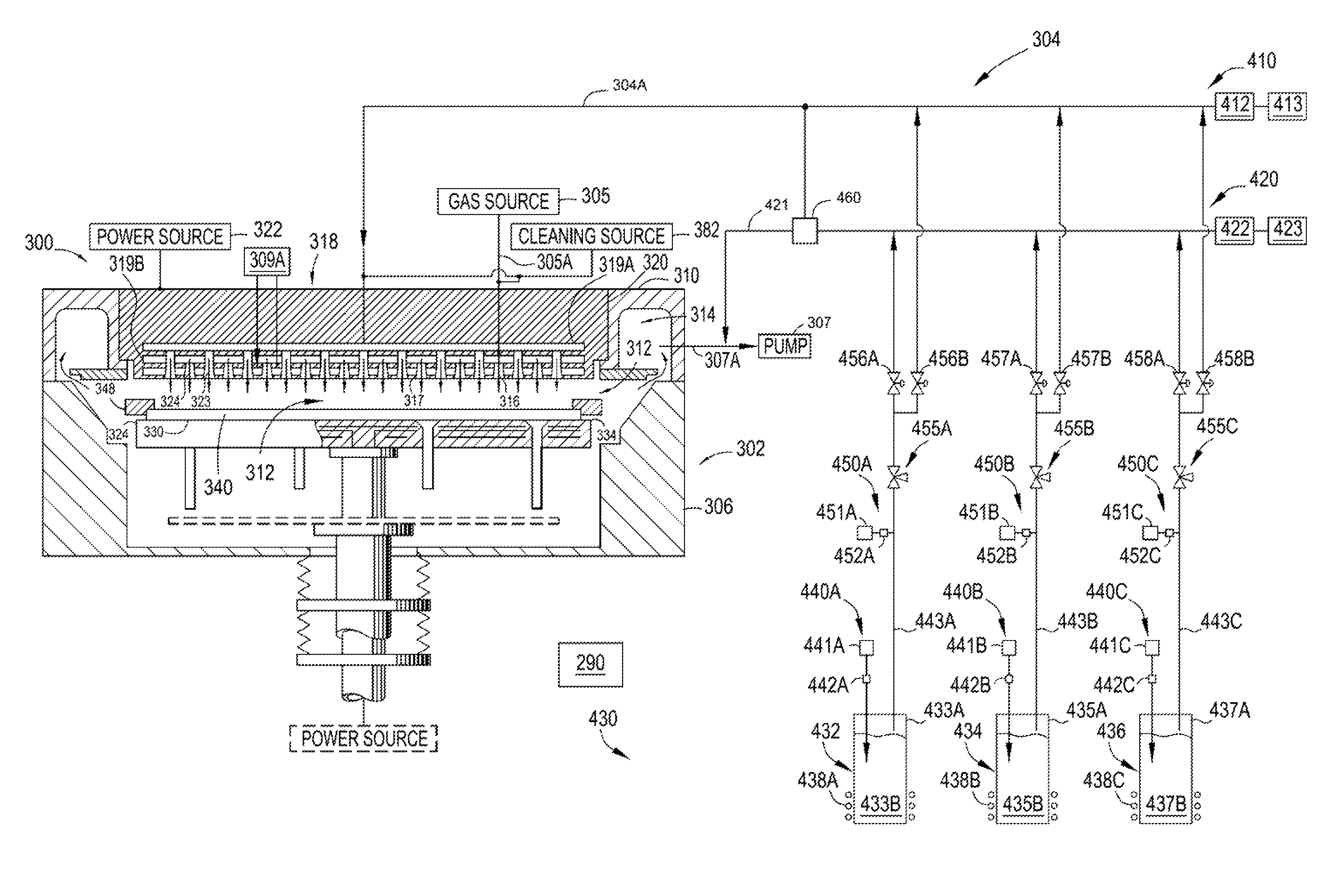
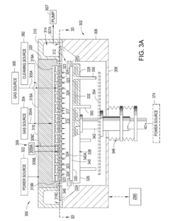
Apparatus and method of forming an indium gallium zinc oxide layer
PatentActiveUS9214340B2
Innovation
- A method and apparatus for forming a multi-element containing film using a gas distribution plate assembly with a precursor plenum and heat exchanging channel, allowing for precise control of precursor gas flow and composition, enabling the deposition of IGZO layers with tailored stoichiometry and reduced environmental exposure.
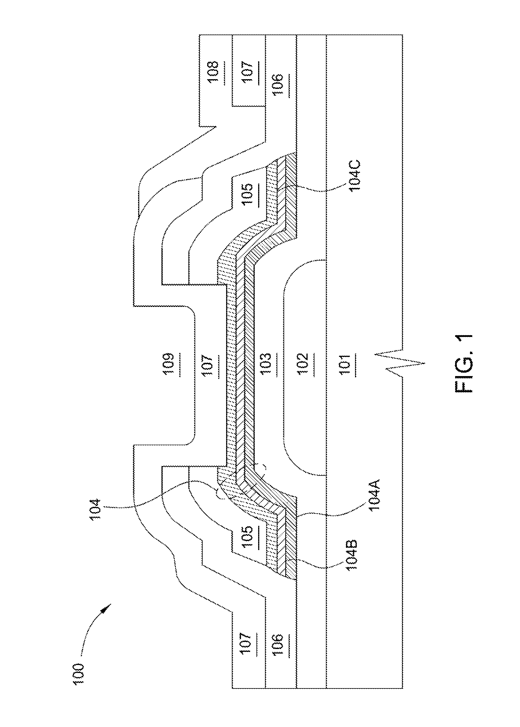
Manufacturing method of thin film transistor
PatentActiveUS8647932B2
Innovation
- A thin film transistor with a double-layer electrode structure, where the seed layer is formed of indium gallium zinc oxide (IGZO) doped transparent conductive material and the main layer is made of transparent conductive materials like indium tin oxide (ITO), zinc oxide (ZnO), or tin oxide (SnO2), reducing contact resistance through a deposition and thermal annealing process.
Materials Compatibility and Interface Engineering Challenges
The integration of IGZO (Indium Gallium Zinc Oxide) thin films with organic electronics presents significant materials compatibility and interface engineering challenges that must be addressed for successful device fabrication. The fundamental issue stems from the inherent differences in material properties between inorganic IGZO semiconductors and organic electronic components, creating complex interface dynamics that affect overall device performance.
One primary challenge is the surface energy mismatch between IGZO and organic materials. IGZO typically exhibits higher surface energy compared to most organic semiconductors, leading to poor wetting and adhesion issues during fabrication processes. This incompatibility can result in delamination, interface voids, and inconsistent film formation, ultimately compromising device reliability and performance characteristics.
Chemical compatibility represents another critical concern. IGZO processing often involves oxygen-rich environments and high-temperature annealing steps that can degrade organic materials through oxidation or thermal decomposition. Conversely, organic solvents used in the deposition of organic layers may cause etching or modification of the IGZO surface, altering its electronic properties and creating unwanted interface states that trap charge carriers.
The electronic band alignment between IGZO and organic materials presents a sophisticated engineering challenge. Misalignment of energy levels creates barriers to charge transport across interfaces, resulting in voltage losses and reduced device efficiency. This issue is particularly pronounced in hybrid devices such as organic-inorganic photodetectors or transistors where efficient charge transfer across the interface is essential for proper functionality.
Interface stability over time poses additional concerns for commercial applications. Environmental factors such as humidity, temperature fluctuations, and light exposure can accelerate degradation processes at the IGZO-organic interface. This degradation often manifests as increasing contact resistance, threshold voltage shifts in transistors, or decreasing quantum efficiency in photovoltaic applications.
Recent research has explored several promising approaches to address these challenges, including the use of buffer layers to mediate surface energy differences, low-temperature processing techniques compatible with both material systems, and surface modification strategies to improve adhesion and electronic coupling. Self-assembled monolayers (SAMs) have shown particular promise in modifying IGZO surfaces to improve compatibility with subsequently deposited organic layers.
Advanced interface engineering techniques, such as gradient composition layers and controlled atmosphere processing, are emerging as potential solutions to overcome the fundamental materials incompatibilities while preserving the advantageous properties of both IGZO and organic electronic components.
Sustainability and Environmental Impact of IGZO-Organic Hybrid Devices
The integration of IGZO thin films with organic electronics presents significant sustainability advantages compared to conventional semiconductor technologies. IGZO-organic hybrid devices utilize abundant materials like indium, gallium, zinc, and oxygen, reducing dependence on scarce resources. These devices can be manufactured using low-temperature processes (typically below 300°C), resulting in substantially lower energy consumption compared to traditional silicon-based technologies that require processing temperatures exceeding 1000°C.
Environmental benefits extend throughout the product lifecycle. The reduced processing temperatures enable the use of flexible plastic substrates rather than rigid silicon wafers, decreasing material waste and enabling novel form factors. Additionally, IGZO-organic hybrid devices demonstrate excellent power efficiency during operation, with IGZO transistors requiring minimal power in standby mode due to their ultra-low leakage currents.
Life cycle assessments indicate that IGZO-organic hybrid devices generate approximately 40-60% less carbon emissions during manufacturing compared to equivalent silicon-based electronics. The potential for biodegradable organic components further enhances end-of-life sustainability, though challenges remain in developing fully biodegradable electronic systems that maintain performance standards.
Recycling considerations present both opportunities and challenges. While the organic components may be biodegradable, the recovery of indium—a relatively scarce element—remains important. Current research focuses on developing efficient recycling methods for IGZO components, with hydrometallurgical processes showing promise for indium recovery rates exceeding 85%.
Regulatory frameworks are evolving to address these novel materials. The European Union's Restriction of Hazardous Substances (RoHS) and Waste Electrical and Electronic Equipment (WEEE) directives increasingly influence manufacturing standards, with IGZO-organic hybrids generally aligning well with these requirements due to their reduced toxic material content.
Future sustainability improvements focus on several key areas: developing indium-free alternatives using more abundant elements; enhancing manufacturing efficiency to further reduce energy consumption; extending device lifespans through improved stability; and creating closed-loop recycling systems. Research at institutions including Stanford University and the University of Tokyo demonstrates progress toward fully recyclable or biodegradable electronic components that maintain the performance advantages of IGZO-organic hybrid systems.
Unlock deeper insights with Patsnap Eureka Quick Research — get a full tech report to explore trends and direct your research. Try now!
Generate Your Research Report Instantly with AI Agent
Supercharge your innovation with Patsnap Eureka AI Agent Platform!