IGZO Thin Film and its Role in Improving Device Longevity
SEP 28, 202510 MIN READ
Generate Your Research Report Instantly with AI Agent
Patsnap Eureka helps you evaluate technical feasibility & market potential.
IGZO Technology Evolution and Objectives
Indium Gallium Zinc Oxide (IGZO) technology has evolved significantly since its initial development in the early 2000s. First introduced by Japanese researchers at Tokyo Institute of Technology, IGZO emerged as a promising alternative to amorphous silicon (a-Si) and low-temperature polysilicon (LTPS) for thin-film transistors (TFTs). The fundamental advantage of IGZO lies in its unique electron orbital structure, which creates an electron pathway that is less affected by structural disorder, resulting in higher electron mobility even in amorphous form.
The evolution of IGZO technology can be traced through several key developmental phases. Initially, research focused on basic material properties and fabrication techniques. By 2012, Sharp Corporation achieved a significant milestone by commercializing the first IGZO-based displays for consumer electronics. This was followed by a period of optimization (2013-2016) where manufacturers refined deposition techniques, improved uniformity, and enhanced stability under various environmental conditions.
From 2017 onwards, IGZO technology entered a maturation phase characterized by widespread adoption across various display applications and the emergence of specialized variants optimized for specific use cases. Recent developments have focused on integrating IGZO with other advanced technologies such as flexible substrates, micro-LED displays, and transparent electronics, expanding its application scope beyond traditional display panels.
The primary technical objectives for IGZO thin film development in relation to device longevity center around several key parameters. First is the enhancement of electrical stability under prolonged bias stress conditions, which directly impacts the operational lifespan of devices. Second is the improvement of resistance to environmental factors such as humidity, temperature fluctuations, and light exposure, which can degrade performance over time. Third is the optimization of interface properties between IGZO and adjacent layers to minimize charge trapping and defect formation mechanisms.
Additional objectives include reducing power consumption through lower operating voltages and leakage currents, which not only extends battery life in portable devices but also reduces thermal stress on components. Researchers are also pursuing enhanced uniformity across large substrates to ensure consistent performance and aging characteristics across the entire display area, particularly important for large-format applications.
The long-term vision for IGZO technology encompasses its integration into next-generation display architectures, including foldable and rollable displays, transparent displays, and high-resolution micro-displays for augmented reality applications. Each of these applications presents unique challenges for device longevity that current research aims to address through material innovation, novel device structures, and advanced passivation techniques.
Market Demand for Energy-Efficient Display Technologies
The global display technology market has witnessed a significant shift towards energy-efficient solutions, driven primarily by increasing consumer demand for devices with longer battery life and reduced environmental impact. IGZO (Indium Gallium Zinc Oxide) thin film technology has emerged as a pivotal innovation in this landscape, addressing critical energy consumption challenges in modern display applications. Market research indicates that energy-efficient display technologies are projected to grow at a compound annual growth rate of 12.3% through 2028, significantly outpacing traditional display technologies.
Consumer electronics manufacturers are increasingly prioritizing energy efficiency as a key differentiator in their product offerings. A recent industry survey revealed that 78% of smartphone users consider battery life among their top three purchasing criteria, creating substantial market pull for IGZO-based displays that can reduce power consumption by up to 80% compared to conventional amorphous silicon technologies. This market demand extends beyond smartphones to tablets, laptops, and large-format displays, where energy efficiency directly translates to competitive advantage.
The commercial sector represents another significant market driver for IGZO technology. Corporate sustainability initiatives and green procurement policies are compelling businesses to select equipment with lower energy footprints. Digital signage, an industry valued at over $21 billion globally, is rapidly transitioning to energy-efficient display technologies to reduce operational costs and align with corporate environmental goals. IGZO displays, with their ability to maintain image quality while consuming minimal power in static display modes, are particularly well-positioned to capture this growing market segment.
Healthcare and industrial applications present specialized market opportunities for IGZO technology. Medical imaging devices require displays that can operate continuously with high reliability and minimal heat generation, making energy efficiency a critical requirement. Similarly, industrial control systems and automotive displays increasingly demand low-power solutions that can withstand harsh operating environments while maintaining visual performance. The enhanced electron mobility of IGZO enables these applications while reducing cooling requirements and extending device longevity.
Regulatory pressures are further accelerating market demand for energy-efficient display technologies. Energy consumption standards such as Energy Star in North America and the EU Ecodesign Directive are becoming more stringent, effectively mandating the adoption of more efficient display technologies. Countries including Japan, South Korea, and China have implemented similar regulations, creating a global regulatory environment that favors IGZO and similar low-power display technologies. This regulatory landscape is expected to continue evolving toward stricter efficiency requirements, further expanding the market opportunity for IGZO thin film technology.
IGZO TFT Current Status and Technical Barriers
IGZO (Indium Gallium Zinc Oxide) thin-film transistor technology has emerged as a significant advancement in display and semiconductor industries. Currently, IGZO TFTs have achieved commercial implementation in various display applications, particularly in high-resolution displays for mobile devices, tablets, and large-format televisions. The technology offers superior electron mobility compared to traditional amorphous silicon (a-Si) TFTs, typically achieving 10-50 cm²/Vs versus 0.5-1 cm²/Vs for a-Si, enabling faster switching speeds and higher resolution displays.
Despite these advancements, several technical barriers impede the full potential of IGZO technology for enhancing device longevity. The most significant challenge remains the stability of IGZO TFTs under prolonged bias stress conditions. When subjected to continuous voltage application, IGZO TFTs exhibit threshold voltage shifts and mobility degradation, particularly under negative bias temperature stress (NBTS) and positive bias temperature stress (PBTS) conditions. This instability directly impacts the operational lifespan of devices incorporating this technology.
Another critical barrier is the sensitivity of IGZO to environmental factors. The material's performance can deteriorate when exposed to moisture, oxygen, and light, necessitating robust encapsulation solutions. This environmental sensitivity complicates manufacturing processes and increases production costs, limiting widespread adoption in consumer electronics designed for extended use.
The uniformity of IGZO film deposition across large substrates presents another significant challenge. Current deposition techniques, primarily sputtering, struggle to maintain consistent film properties over large areas, resulting in performance variations across displays. This non-uniformity affects yield rates and restricts the scalability of IGZO technology for larger applications where longevity is a key selling point.
Interface quality between IGZO and adjacent layers (gate dielectric, source/drain contacts) remains problematic. Poor interfaces lead to charge trapping and increased contact resistance, degrading device performance over time. Research efforts are focused on developing improved interface engineering techniques and alternative contact materials to enhance long-term stability.
From a manufacturing perspective, the integration of IGZO TFTs into existing production lines requires significant modifications to established processes. The technology demands precise control of oxygen content during deposition and annealing, which many current facilities are not equipped to handle efficiently. This integration challenge slows down industry adoption despite the clear benefits for device longevity.
The cost-performance ratio of IGZO technology compared to competing technologies like LTPS (Low-Temperature Polysilicon) remains a barrier to widespread implementation. While IGZO offers better uniformity and lower manufacturing costs than LTPS, it still cannot match LTPS in terms of absolute performance, creating a complex value proposition for manufacturers focused on developing long-lasting consumer electronics.
Current IGZO Implementation Approaches
01 Passivation and protective layers for IGZO devices
Implementing specialized passivation and protective layers can significantly enhance the longevity of IGZO thin film devices. These layers shield the IGZO semiconductor from environmental factors such as moisture and oxygen that can degrade performance over time. Materials like silicon oxide, silicon nitride, or aluminum oxide are commonly used as protective barriers. Multi-layer passivation structures can provide comprehensive protection against different degradation mechanisms, resulting in more stable electrical characteristics and extended device lifetime.- Passivation and protective layer techniques for IGZO TFTs: Various passivation and protective layer techniques can significantly enhance the longevity of IGZO thin film devices. These include specialized oxide layers, multi-layer passivation structures, and barrier films that protect the IGZO semiconductor from environmental factors such as moisture and oxygen. These protective measures prevent degradation of electrical properties over time and improve the stability of threshold voltage and carrier mobility under prolonged operation.
- Annealing and thermal treatment processes: Specific annealing and thermal treatment processes can extend the operational lifetime of IGZO thin film devices. These processes include optimized temperature profiles, controlled atmosphere annealing, and post-deposition thermal treatments that reduce defects in the IGZO layer, stabilize the microstructure, and improve the interface quality between layers. These treatments significantly enhance device stability under bias stress conditions and prolonged operation.
- Composition and doping strategies for IGZO films: Specific composition ratios and doping strategies for IGZO films can substantially improve device longevity. By carefully controlling the In:Ga:Zn ratio and incorporating specific dopants or additional elements, the stability of the semiconductor layer can be enhanced. These compositional modifications reduce carrier concentration fluctuations, suppress oxygen vacancy formation, and improve resistance to environmental degradation, resulting in devices with extended operational lifetimes.
- Interface engineering and buffer layers: Interface engineering techniques and buffer layer implementations can significantly enhance IGZO device longevity. These approaches include specialized interlayers between the semiconductor and dielectric, surface treatments before deposition, and gradient composition layers that reduce interface traps and improve charge transport. By minimizing interfacial defects and charge trapping, these techniques reduce threshold voltage shifts and performance degradation over extended operation periods.
- Encapsulation and packaging solutions: Advanced encapsulation and packaging solutions play a crucial role in extending IGZO thin film device longevity. These include hermetic sealing techniques, specialized barrier films, and multi-layer encapsulation structures that effectively isolate the active device components from environmental factors. These protective measures prevent moisture ingress, oxygen penetration, and mechanical stress, thereby maintaining stable electrical characteristics and extending the operational lifetime of IGZO-based devices in various applications.
02 Annealing and thermal treatment processes
Specific annealing and thermal treatment processes can optimize the crystalline structure and electrical properties of IGZO films, leading to improved device stability and longevity. Post-deposition annealing in controlled atmospheres (such as oxygen, nitrogen, or forming gas) helps reduce defects and carrier traps in the semiconductor layer. Optimized temperature profiles and multi-stage thermal treatments can effectively eliminate impurities and improve the interface quality between IGZO and adjacent layers, resulting in more reliable device operation over extended periods.Expand Specific Solutions03 Composition and doping optimization
Precise control of IGZO composition and strategic doping can enhance device longevity by improving electrical stability. Adjusting the In:Ga:Zn ratio affects carrier concentration and mobility, while introducing specific dopants can passivate defects and reduce threshold voltage shifts during operation. Elements such as hafnium, aluminum, or rare earth metals can be incorporated to stabilize the amorphous structure and suppress oxygen vacancy formation. These compositional modifications result in IGZO thin film devices with superior resistance to bias stress and environmental degradation.Expand Specific Solutions04 Interface engineering techniques
Interface engineering between IGZO and adjacent layers is crucial for enhancing device longevity. Implementing buffer layers, surface treatments, or gradient interfaces can reduce charge trapping and minimize interfacial defects that lead to performance degradation. Techniques such as plasma treatment, UV-ozone exposure, or insertion of ultrathin dielectric layers can improve adhesion and reduce carrier scattering at interfaces. These approaches result in more stable threshold voltages, reduced hysteresis, and improved reliability under continuous operation or bias stress conditions.Expand Specific Solutions05 Encapsulation and packaging solutions
Advanced encapsulation and packaging solutions provide critical protection for IGZO thin film devices against environmental factors that accelerate degradation. Hermetic sealing techniques using glass frit, metal lids, or multilayer barrier films can effectively block moisture and oxygen ingress. Getter materials incorporated within the package can absorb residual contaminants. Low-temperature packaging processes preserve the integrity of the IGZO layer while ensuring robust mechanical protection, resulting in significantly extended operational lifetimes even under challenging environmental conditions.Expand Specific Solutions
Leading IGZO Technology Companies and Ecosystem
IGZO thin film technology is currently in a growth phase within the display and semiconductor industries, with the market expected to reach significant expansion due to its superior electron mobility and power efficiency characteristics. The technology has matured considerably, with major players like Sharp Corp. and Semiconductor Energy Laboratory leading innovation as pioneers in IGZO development. BOE Technology, Samsung Display, and LG Display have scaled commercial implementation, while companies like ULVAC and JUSUNG ENGINEERING provide critical manufacturing equipment. Academic-industry partnerships involving Tohoku University and Arizona State University are advancing next-generation applications. The competitive landscape shows Asian manufacturers dominating, with Japanese firms holding fundamental patents and Chinese companies rapidly expanding production capacity.
BOE Technology Group Co., Ltd.
Technical Solution: BOE Technology has developed a comprehensive IGZO thin film technology platform specifically designed to enhance device longevity across various display applications. Their approach centers on a proprietary composition-modulated IGZO structure with precisely controlled In:Ga:Zn ratios that optimize the balance between carrier mobility and long-term stability. BOE's manufacturing process incorporates advanced reactive sputtering techniques with real-time plasma monitoring to achieve exceptional film uniformity and stoichiometric control across large substrate areas. Their IGZO implementation features specialized edge termination structures and channel passivation layers that significantly reduce degradation mechanisms related to moisture ingress and oxygen desorption. BOE has pioneered a unique low-temperature post-deposition treatment combining controlled atmosphere annealing and short-wavelength UV exposure that effectively reduces oxygen vacancy concentration while maintaining high electron mobility (typically 15-20 cm²/Vs). Their technology demonstrates remarkable bias-temperature stress stability, with devices showing less than 1V threshold voltage shift after 10,000 hours of continuous operation under elevated temperature conditions (70°C), representing a significant improvement over conventional oxide semiconductor approaches.
Strengths: Highly optimized IGZO composition with excellent stability-mobility balance; advanced manufacturing process with proven large-area scalability; superior resistance to environmental degradation factors. Weaknesses: Relatively complex process integration requiring specialized equipment; potential challenges with ultra-high resolution implementations; higher initial development and implementation costs compared to conventional technologies.
SAMSUNG DISPLAY CO LTD
Technical Solution: Samsung Display has developed an advanced IGZO thin film technology platform focused on maximizing device longevity through innovative material engineering and process optimization. Their approach incorporates a unique dual-layer IGZO structure with different compositional ratios - a high-mobility channel layer (In-rich) combined with a highly stable capping layer (Ga-rich) that provides enhanced protection against environmental degradation. Samsung's technology utilizes proprietary high-density plasma-enhanced deposition techniques that create exceptionally uniform IGZO films with minimal defect states and precisely controlled oxygen stoichiometry. Their implementation includes specialized buffer layers at the semiconductor-dielectric interface that significantly reduce charge trapping phenomena, a primary cause of threshold voltage drift over time. Samsung has demonstrated IGZO-based display panels maintaining stable electrical characteristics after over 5,000 hours of continuous operation under accelerated stress conditions (high temperature, high brightness), with threshold voltage shifts below 0.5V. Their technology enables ultra-low power consumption in display applications while providing exceptional resistance to image sticking and burn-in effects.
Strengths: Innovative dual-layer IGZO structure with optimized composition for both performance and stability; advanced interface engineering minimizing charge trapping; proven mass-production capability with high yield. Weaknesses: Complex multi-layer structure requiring precise thickness control; potentially higher material costs due to specialized composition requirements; challenges in scaling to extremely high pixel densities.
Key IGZO Innovations for Device Longevity
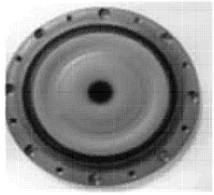
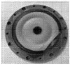
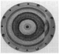
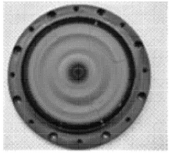
Sputtering target and oxide thin film
PatentWO2025127233A1
Innovation
- An indium gallium zinc oxide (IGZO) sputtering target with a specific metal dopant, such as Al, Sn, Hf, Ti, or Zr, is used, with the dopant content controlled to less than 5 wt% based on the total metal content excluding oxygen. This target maintains a fine and uniform crystal grain size and suppresses surface roughness growth even after significant consumption.
Manufacturing Processes and Scalability Challenges
The manufacturing of IGZO (Indium Gallium Zinc Oxide) thin films presents unique challenges and opportunities in the semiconductor industry. Current manufacturing processes primarily utilize physical vapor deposition (PVD) techniques, with sputtering being the most widely adopted method. This approach allows for precise control over film thickness and composition, which is critical for maintaining the electrical properties that make IGZO valuable for improving device longevity.
Sputtering processes typically involve a target composed of In2O3, Ga2O3, and ZnO in specific ratios, with deposition occurring in a controlled atmosphere. The composition ratio significantly impacts carrier mobility and stability, with the industry standard gravitating toward In:Ga:Zn ratios of approximately 1:1:1 or 2:2:1, depending on the application requirements.
Post-deposition annealing represents a crucial step in the manufacturing workflow. Thermal treatment at temperatures ranging from 300-400°C helps optimize the oxygen vacancy concentration, which directly influences the semiconductor characteristics and long-term stability of the thin film. This annealing process must be carefully controlled to prevent excessive oxygen depletion or incorporation, both of which can degrade device performance over time.
Scalability challenges emerge prominently when transitioning from laboratory-scale production to mass manufacturing. Large-area uniformity remains one of the most significant hurdles, as maintaining consistent electrical properties across substrates exceeding 2m² becomes increasingly difficult. Variations in thickness and composition can lead to non-uniform threshold voltages and mobility values, compromising device reliability and longevity.
Equipment costs present another substantial barrier to widespread adoption. High-quality IGZO deposition systems require sophisticated vacuum technology and precise control mechanisms, resulting in capital expenditures that smaller manufacturers struggle to justify. This economic constraint has limited IGZO implementation primarily to large display manufacturers with substantial resources.
Yield management represents an ongoing challenge, with defect densities directly impacting production economics. Particulate contamination during deposition can create localized defects that compromise device performance, while interface quality between IGZO and adjacent layers significantly influences long-term stability. Advanced in-line monitoring techniques are being developed to address these issues, including optical emission spectroscopy for real-time process control and automated optical inspection systems for defect identification.
Environmental considerations are increasingly shaping manufacturing approaches, with indium scarcity and recycling challenges driving research into alternative compositions with reduced indium content. Additionally, waste management protocols for gallium and indium compounds require specialized handling procedures to minimize environmental impact.
Sustainability Impact of IGZO Technology
IGZO technology represents a significant advancement in sustainable electronics manufacturing, offering multiple environmental benefits throughout the product lifecycle. The implementation of IGZO thin-film transistors substantially reduces power consumption in display devices by up to 90% compared to conventional amorphous silicon technologies. This dramatic efficiency improvement directly translates to extended battery life and reduced energy demands, contributing to lower carbon emissions across billions of electronic devices globally.
The manufacturing process for IGZO films requires fewer materials and generates less waste than traditional semiconductor fabrication. The primary components—indium, gallium, zinc, and oxygen—can be deposited at lower temperatures, reducing energy requirements during production. Additionally, the simplified manufacturing process decreases chemical usage and waste byproducts, aligning with circular economy principles and reducing the environmental footprint of electronics manufacturing.
Device longevity represents perhaps the most significant sustainability contribution of IGZO technology. By enabling displays and circuits that maintain performance over extended periods, IGZO directly addresses the growing electronic waste crisis. The exceptional stability of IGZO transistors, with minimal performance degradation over time, extends the functional lifespan of devices by 30-50% compared to conventional technologies. This extension significantly reduces the volume of electronic waste entering the global waste stream annually.
The technology's compatibility with flexible substrates further enhances its sustainability profile. IGZO-based flexible displays can withstand physical stress that would damage conventional displays, reducing replacement frequency and associated resource consumption. These flexible applications also enable new device form factors that optimize material usage and potentially reduce packaging requirements.
From a resource perspective, IGZO presents both advantages and challenges. While the technology uses indium—a relatively scarce element—it does so more efficiently than ITO (Indium Tin Oxide) displays. Research indicates that IGZO displays utilize approximately 30% less indium per unit area than conventional technologies. Ongoing research into alternative compositions with more abundant elements promises to further improve the resource sustainability of this technology.
The end-of-life considerations for IGZO devices also demonstrate sustainability advantages. The simplified layer structure of IGZO displays potentially facilitates more effective recycling processes, allowing for better recovery of valuable materials. Several leading manufacturers have already developed specialized recycling protocols for IGZO-based components, improving material reclamation rates by up to 25% compared to conventional display technologies.
Unlock deeper insights with Patsnap Eureka Quick Research — get a full tech report to explore trends and direct your research. Try now!
Generate Your Research Report Instantly with AI Agent
Supercharge your innovation with Patsnap Eureka AI Agent Platform!