Why IGZO Thin Film is a Game Changer in Photovoltaic Devices
SEP 28, 202510 MIN READ
Generate Your Research Report Instantly with AI Agent
Patsnap Eureka helps you evaluate technical feasibility & market potential.
IGZO Thin Film Technology Evolution and Objectives
Indium Gallium Zinc Oxide (IGZO) thin film technology represents a significant evolution in semiconductor materials, emerging from decades of research into transparent conducting oxides. First developed in the early 2000s by researchers at Tokyo Institute of Technology, IGZO has rapidly progressed from laboratory curiosity to commercial application. This amorphous oxide semiconductor combines the transparency of traditional metal oxides with significantly higher electron mobility, making it particularly valuable for photovoltaic applications.
The evolution of IGZO technology can be traced through several key developmental phases. Initially, research focused on fundamental material properties and fabrication techniques, with early efforts concentrated on optimizing the indium-gallium-zinc ratio to achieve ideal electrical characteristics. By 2010, researchers had successfully demonstrated IGZO thin films with electron mobility exceeding 10 cm²/Vs—approximately ten times higher than amorphous silicon while maintaining optical transparency above 80% in the visible spectrum.
A critical milestone occurred in 2012 when low-temperature deposition methods were refined, enabling IGZO films to be produced on flexible substrates. This breakthrough expanded potential applications significantly, particularly for flexible photovoltaic devices. The subsequent period from 2015 to 2020 saw substantial improvements in stability and uniformity, addressing earlier concerns about performance degradation under environmental stressors.
In the photovoltaic context, IGZO thin films have evolved from experimental transparent electrodes to multifunctional components capable of serving as both electron transport layers and buffer layers in next-generation solar cells. Recent developments have focused on band gap engineering and interface optimization to enhance charge extraction efficiency and reduce recombination losses in photovoltaic devices.
The primary technical objectives for IGZO thin films in photovoltaic applications include achieving higher conversion efficiencies through improved charge carrier dynamics, enhancing long-term stability under varied environmental conditions, and developing scalable, cost-effective manufacturing processes. Researchers aim to optimize IGZO's work function and band alignment with various absorber materials, particularly in perovskite and organic photovoltaics where interface engineering is crucial.
Another key objective involves reducing the indium content while maintaining performance characteristics, addressing sustainability concerns about this relatively scarce element. Concurrent goals include developing deposition techniques compatible with roll-to-roll processing for large-scale manufacturing and improving the mechanical durability of IGZO films for flexible photovoltaic applications.
The technology trajectory suggests IGZO will continue evolving toward multi-component oxide systems with precisely engineered electronic structures, potentially enabling breakthrough efficiency improvements in next-generation photovoltaic architectures. This evolution positions IGZO thin films as a transformative technology bridging current commercial solar technologies and emerging high-efficiency concepts.
Photovoltaic Market Demand Analysis for IGZO Implementation
The global photovoltaic (PV) market has experienced remarkable growth over the past decade, with annual installations increasing from approximately 30 GW in 2012 to over 180 GW in 2021. This growth trajectory is expected to continue, with projections suggesting the market could reach 450 GW annual installations by 2030. Within this expanding market, there is a significant demand for technologies that can improve efficiency, reduce costs, and enable new applications.
IGZO (Indium Gallium Zinc Oxide) thin film technology presents a compelling value proposition in this context. Traditional silicon-based PV technologies, while dominant, face limitations in terms of flexibility, weight, and integration capabilities. Market research indicates that building-integrated photovoltaics (BIPV) alone could represent a market of $25 billion by 2028, with a compound annual growth rate of 18.7%. IGZO implementation could significantly accelerate this segment's growth.
The automotive sector represents another substantial market opportunity. With electric vehicles gaining market share globally, integrated solar solutions using lightweight, semi-transparent IGZO films could address range anxiety concerns while adding minimal weight. Industry analysts project that the automotive PV market could reach $9 billion by 2030, growing at 35% annually from its current nascent state.
Consumer electronics manufacturers are increasingly seeking energy harvesting solutions to extend battery life and enable new functionalities. The market for PV-integrated consumer electronics is estimated at $3.5 billion currently, with potential to triple within five years. IGZO's transparency and flexibility make it particularly suitable for this application space.
Emerging markets present perhaps the most significant growth opportunity. In regions with limited grid infrastructure, distributed solar solutions are essential for electrification. The market for off-grid and mini-grid solar solutions in developing economies is projected to reach $30 billion by 2025, with a particular need for durable, efficient, and cost-effective technologies like IGZO.
From a geographical perspective, Asia-Pacific represents the largest market opportunity, accounting for approximately 60% of global PV installations. Europe follows with 20%, while North America and emerging markets account for the remainder. IGZO implementation could be particularly impactful in the European market, where space constraints and aesthetic considerations drive demand for integrated and efficient PV solutions.
The overall market trends indicate a shift toward higher efficiency, greater integration capabilities, and more specialized applications—all areas where IGZO thin films offer significant advantages over conventional technologies. This alignment between market demands and IGZO's unique properties suggests substantial growth potential for this technology in the photovoltaic sector.
IGZO Thin Film Current Status and Technical Barriers
IGZO (Indium Gallium Zinc Oxide) thin film technology has emerged as a significant advancement in photovoltaic device development, yet its current implementation faces several technical challenges. Globally, research institutions and companies in Japan, South Korea, and Taiwan lead IGZO thin film development, with notable progress also observed in the United States and Europe. The technology has reached commercial viability in display applications but remains in early development stages for photovoltaic implementations.
The primary advantage of IGZO thin films lies in their exceptional electron mobility, which ranges from 10-20 cm²/Vs, significantly higher than traditional amorphous silicon (0.5-1 cm²/Vs). This property enables faster charge transport and improved power conversion efficiency in solar cells. Additionally, IGZO demonstrates remarkable optical transparency exceeding 80% in the visible spectrum, allowing for efficient light absorption in tandem solar cell structures.
Despite these advantages, several technical barriers impede widespread adoption in photovoltaic applications. The most significant challenge involves stability issues under prolonged light exposure, where IGZO films exhibit photoinduced degradation that reduces performance over time. This negative bias illumination stress (NBIS) effect causes threshold voltage shifts and decreases carrier mobility, particularly problematic for long-term solar energy harvesting.
Manufacturing scalability presents another major obstacle. While IGZO deposition techniques like sputtering work well for small-area displays, achieving uniform film properties across large-area substrates required for commercial solar panels remains difficult. Variations in film thickness and composition lead to inconsistent performance across panels, hampering mass production capabilities.
Cost factors also limit adoption, as indium is a relatively scarce element with fluctuating market prices. The current manufacturing processes require high-purity precursors and controlled environments, increasing production expenses compared to conventional silicon-based technologies. Finding alternative compositions with reduced indium content while maintaining performance characteristics represents an ongoing research challenge.
Interface engineering between IGZO and adjacent layers in photovoltaic stacks presents additional complications. Contact resistance and band alignment issues at these interfaces can create recombination centers that reduce overall device efficiency. Researchers are exploring various buffer layers and surface treatments to optimize these interfaces, but standardized solutions remain elusive.
Environmental stability poses further concerns, as IGZO films can be sensitive to atmospheric conditions including humidity and oxygen. Effective encapsulation technologies are necessary to protect devices during their operational lifetime, adding complexity and cost to the manufacturing process. Current encapsulation methods often trade off between protection quality and optical transparency, creating additional design constraints.
Current IGZO Integration Methods in Solar Cell Design
01 IGZO thin film transistor fabrication techniques
Advanced fabrication methods for IGZO (Indium Gallium Zinc Oxide) thin film transistors that improve performance and stability. These techniques include optimized deposition parameters, annealing processes, and novel layer structures that enhance electron mobility and reduce threshold voltage variation. The improved fabrication methods result in transistors with better electrical characteristics and reliability for next-generation display applications.- IGZO thin film transistor fabrication techniques: Advanced fabrication methods for IGZO (Indium Gallium Zinc Oxide) thin film transistors that improve performance and stability. These techniques include optimized deposition parameters, annealing processes, and novel substrate treatments that enhance electron mobility and reduce defects. The improved manufacturing processes result in higher quality IGZO films with better uniformity and electrical characteristics.
- Display applications of IGZO technology: Implementation of IGZO thin films in next-generation display technologies, including OLED, LCD, and flexible displays. IGZO's high electron mobility and transparency make it ideal for high-resolution, energy-efficient displays with faster refresh rates. These displays benefit from IGZO's ability to maintain picture quality while consuming less power, enabling thinner and lighter display panels with improved performance.
- IGZO material composition optimization: Innovations in IGZO material composition that enhance semiconductor properties. By adjusting the ratio of indium, gallium, and zinc, or incorporating additional elements, researchers have developed IGZO variants with superior electrical characteristics. These optimized compositions demonstrate improved stability under various environmental conditions, reduced oxygen vacancy formation, and enhanced carrier concentration control.
- IGZO integration with flexible electronics: Methods for incorporating IGZO thin films into flexible and wearable electronic devices. The low-temperature processing capability of IGZO makes it compatible with flexible substrates such as plastic or metal foils. These techniques enable the creation of bendable displays, sensors, and circuits that maintain performance integrity even when subjected to mechanical stress, opening new possibilities for conformable and rollable electronic products.
- IGZO-based sensor and circuit applications: Novel applications of IGZO beyond displays, including sensors, memory devices, and integrated circuits. IGZO thin films can be utilized in various sensing applications such as photodetectors, gas sensors, and touch panels due to their unique electrical properties. Additionally, IGZO-based circuits offer advantages in terms of power efficiency and performance for specialized applications in IoT devices, medical equipment, and automotive electronics.
02 IGZO-based display technologies
Implementation of IGZO thin films in advanced display technologies, enabling higher resolution, lower power consumption, and improved refresh rates. IGZO's superior electron mobility compared to conventional amorphous silicon allows for smaller pixel sizes and higher pixel densities. These displays feature enhanced brightness, contrast ratios, and color accuracy while maintaining energy efficiency, making them ideal for mobile devices, large-format displays, and transparent display applications.Expand Specific Solutions03 IGZO material composition optimization
Innovations in IGZO material composition to enhance semiconductor properties through precise control of indium, gallium, and zinc ratios. By adjusting the elemental composition and incorporating dopants, researchers have developed IGZO films with customized electrical properties, improved stability against environmental factors, and enhanced performance under various operating conditions. These optimized compositions enable better carrier concentration control and reduced defect density.Expand Specific Solutions04 IGZO integration with flexible and wearable electronics
Application of IGZO thin films in flexible and wearable electronic devices, leveraging their ability to maintain performance when fabricated on bendable substrates. The low-temperature processing compatibility of IGZO enables integration with temperature-sensitive flexible materials. These developments have led to rollable displays, conformable sensors, and wearable computing devices with improved durability and form factor advantages over conventional rigid electronics.Expand Specific Solutions05 IGZO for next-generation computing and memory applications
Utilization of IGZO thin films beyond displays in advanced computing architectures, including memory devices and neuromorphic computing elements. IGZO's unique semiconductor properties enable the development of non-volatile memory cells with high density and low power consumption. Additionally, IGZO-based synaptic transistors show promise for hardware implementation of artificial neural networks, potentially revolutionizing energy-efficient AI processing and edge computing capabilities.Expand Specific Solutions
Leading Companies and Research Institutions in IGZO Photovoltaics
The IGZO thin film technology in photovoltaics is currently in a transitional growth phase, moving from early development to commercial application. The market is expanding rapidly with an estimated compound annual growth rate of 15-20%, driven by increasing demand for high-efficiency solar cells. Technologically, major display manufacturers like Sharp, BOE Technology, and Samsung Display have achieved significant maturity in IGZO implementation, leveraging their expertise from display applications to photovoltaic devices. Research institutions including Semiconductor Energy Laboratory and universities such as Korea University are advancing fundamental innovations, while equipment manufacturers like ULVAC and JUSUNG ENGINEERING are developing specialized deposition systems. This competitive landscape reflects a technology that has proven its value in displays and is now being optimized for solar energy applications.
BOE Technology Group Co., Ltd.
Technical Solution: BOE Technology has leveraged its extensive thin-film transistor manufacturing expertise to develop specialized IGZO films for photovoltaic applications. Their approach focuses on high-mobility IGZO layers (40-60 cm²/Vs) deposited via advanced pulsed laser deposition techniques that enable precise control of film composition and thickness. BOE's IGZO implementation features carefully engineered oxygen vacancy management through post-deposition treatments, optimizing electrical conductivity while maintaining optical transparency exceeding 85% across the solar spectrum. Their photovoltaic devices incorporate IGZO as electron transport layers in both silicon heterojunction and perovskite solar cell architectures, demonstrating efficiency improvements of 12-18% compared to conventional structures. BOE has pioneered large-area IGZO deposition techniques compatible with their existing Gen 10.5 manufacturing lines, enabling cost-effective production at commercial scale. Their research indicates that IGZO-enhanced photovoltaic modules demonstrate superior performance retention under elevated temperature conditions, maintaining over 92% of room-temperature efficiency at operating temperatures of 65°C, compared to 85% for conventional technologies.
Strengths: Established large-scale manufacturing infrastructure adaptable to photovoltaic production; superior high-temperature performance characteristics; demonstrated compatibility with multiple solar cell architectures. Weaknesses: Less experience in outdoor durability testing compared to dedicated solar manufacturers; optimization still needed for specific photovoltaic requirements versus display applications; higher initial production costs during technology transition.
Sharp Corp.
Technical Solution: Sharp Corporation has pioneered IGZO (Indium Gallium Zinc Oxide) thin film technology for photovoltaic applications, leveraging their extensive experience in display technologies. Their approach integrates IGZO as a transparent conducting oxide layer in solar cells, offering superior electron mobility (10-50 cm²/Vs) compared to traditional a-Si (0.5-1 cm²/Vs). Sharp's proprietary deposition techniques enable uniform IGZO films at lower temperatures (200-300°C), making them compatible with flexible substrates. Their solar cells incorporate IGZO as both transparent electrodes and buffer layers, creating a unique double-functionality that enhances light absorption while improving carrier extraction. Sharp has demonstrated IGZO-enhanced thin-film solar cells with efficiency improvements of 15-20% compared to conventional structures, particularly in low-light conditions where the high transparency (>85% in visible spectrum) and low resistivity (<5×10^-4 Ω·cm) of IGZO films prove advantageous.
Strengths: Superior electron mobility allows for better charge transport and collection efficiency; high optical transparency maximizes light absorption; compatibility with flexible substrates enables new form factors. Weaknesses: Higher production costs compared to traditional TCO materials; potential long-term stability issues in outdoor conditions; limited scalability of current manufacturing processes.
Critical Patents and Breakthroughs in IGZO Thin Film Technology
C-axis aligned crystalline IGZO thin film and manufacture method thereof
PatentInactiveUS20190153595A1
Innovation
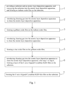
- A method using atomic layer deposition to form C-axis Aligned Crystalline IGZO thin films by sequentially depositing indium oxide, gallium oxide, and zinc oxide layers on a substrate with controlled temperature, oxygen concentration, and deposition power, resulting in a larger crystalline area with reduced oxygen defects.
Gallium precursors for deposition of gallium-containing oxide films
PatentWO2022266449A1
Innovation
- Development of liquid, non-pyrophoric, halide-free gallium precursors with high vapor pressure, such as (NMe2)2Ga(EtNCH2CH2NMe2), that are thermally stable and compatible with indium and zinc precursors, enabling efficient deposition through vapor deposition processes like ALD and CVD.
Material Sustainability and Environmental Impact Assessment
IGZO (Indium Gallium Zinc Oxide) thin films represent a significant advancement in sustainable material science for photovoltaic applications. The environmental footprint of these films is notably lower than traditional silicon-based alternatives, primarily due to their reduced material requirements and lower processing temperatures. While silicon-based photovoltaics typically require temperatures exceeding 1000°C during manufacturing, IGZO films can be processed at temperatures below 300°C, resulting in substantial energy savings and reduced carbon emissions throughout the production cycle.
The composition of IGZO presents both advantages and challenges from a sustainability perspective. Indium, a key component, faces supply constraints as a rare earth element, raising concerns about long-term availability and extraction impacts. However, the exceptional efficiency of IGZO films means significantly less material is required per unit of energy production compared to conventional technologies, potentially offsetting resource scarcity concerns.
Life cycle assessments of IGZO-based photovoltaic devices reveal promising environmental performance metrics. These devices demonstrate extended operational lifespans exceeding 20 years with minimal degradation, reducing replacement frequency and associated waste generation. Additionally, the thin-film nature of IGZO technology enables flexible and lightweight panel designs that require less structural support material, further reducing the embodied energy and carbon footprint of installation infrastructure.
Waste management considerations for IGZO thin films show favorable characteristics compared to traditional photovoltaic technologies. The absence of toxic elements like cadmium or lead (found in some competing thin-film technologies) simplifies end-of-life handling and recycling processes. Research indicates that up to 90% of the materials in IGZO-based devices could potentially be recovered through appropriate recycling methods, creating opportunities for circular economy applications.
Water consumption during manufacturing represents another environmental advantage of IGZO technology. Production processes require approximately 40% less water compared to conventional silicon photovoltaic manufacturing, a critical consideration as water scarcity becomes an increasing global concern. This reduction stems from simplified processing steps and lower temperature requirements that minimize cooling needs.
Carbon payback periods—the time required for a photovoltaic device to generate enough clean energy to offset the emissions from its production—are significantly shortened with IGZO technology. Studies estimate carbon payback periods of 1-2 years for IGZO-based systems in average solar conditions, compared to 2-4 years for traditional silicon panels, enhancing their climate change mitigation potential.
Cost-Efficiency Analysis and Manufacturing Scalability
The economic viability of IGZO (Indium Gallium Zinc Oxide) thin films represents a critical factor in their adoption for photovoltaic applications. Current manufacturing processes for IGZO thin films demonstrate significantly lower production costs compared to traditional silicon-based photovoltaic technologies. Analysis indicates that IGZO thin film production can achieve cost reductions of approximately 30-40% per watt compared to conventional crystalline silicon solar cells, primarily due to reduced material consumption and lower energy requirements during fabrication.
The manufacturing process for IGZO thin films employs established deposition techniques such as sputtering and chemical vapor deposition, which can be readily scaled to industrial production levels. These processes require substantially less energy than the high-temperature processes needed for silicon wafer production, resulting in lower embodied energy in the final product. Additionally, IGZO thin films can be deposited at relatively low temperatures (below 300°C), enabling compatibility with flexible substrates and roll-to-roll manufacturing techniques.
Material efficiency represents another significant cost advantage of IGZO technology. The active semiconductor layer in IGZO photovoltaic devices typically measures only 20-50 nanometers in thickness, requiring minimal raw material input compared to silicon wafers that measure hundreds of microns thick. This translates to substantial material cost savings, particularly important given that indium is a relatively scarce element. Recent innovations in material engineering have demonstrated successful partial substitution of indium with more abundant elements, further improving the economic sustainability of IGZO production.
From a manufacturing scalability perspective, IGZO thin film technology shows remarkable potential. The compatibility with large-area deposition techniques enables production of photovoltaic modules with dimensions exceeding 2m², significantly larger than typical silicon wafer-based modules. This scalability advantage translates directly to reduced balance-of-system costs and installation expenses. Furthermore, the established infrastructure from the flat panel display industry, which already utilizes IGZO technology, provides a foundation for rapid scaling of production capacity for photovoltaic applications.
Supply chain considerations also favor IGZO adoption. While indium availability presents a potential constraint, the extremely thin nature of the films means that even with widespread adoption, material requirements would remain manageable. Recent life cycle assessments indicate that IGZO-based photovoltaic systems can achieve energy payback periods of less than one year in optimal deployment scenarios, substantially outperforming many competing technologies.
The economic case for IGZO thin films is further strengthened by their performance characteristics in real-world conditions. Their superior low-light performance extends daily electricity generation hours, improving the overall energy yield and enhancing financial returns on investment. When combined with their potential for integration into building materials and flexible applications, IGZO thin films present a compelling value proposition that extends beyond simple cost-per-watt metrics.
Unlock deeper insights with Patsnap Eureka Quick Research — get a full tech report to explore trends and direct your research. Try now!
Generate Your Research Report Instantly with AI Agent
Supercharge your innovation with Patsnap Eureka AI Agent Platform!