The Role of Surface Treatment in IGZO Thin Film Capabilities
SEP 28, 20259 MIN READ
Generate Your Research Report Instantly with AI Agent
Patsnap Eureka helps you evaluate technical feasibility & market potential.
IGZO Surface Treatment Background and Objectives
Indium Gallium Zinc Oxide (IGZO) has emerged as a revolutionary material in the field of thin-film transistors (TFTs) since its introduction in the early 2000s. This amorphous oxide semiconductor has gained significant attention due to its superior electron mobility compared to traditional amorphous silicon, while maintaining low production costs and compatibility with existing manufacturing processes. The evolution of IGZO technology has been marked by continuous improvements in performance characteristics, with surface treatment techniques playing an increasingly critical role in enhancing its capabilities.
Surface treatment of IGZO thin films represents a crucial technological frontier that directly impacts device performance, stability, and longevity. Historically, early IGZO implementations suffered from performance inconsistencies, environmental sensitivity, and reliability issues that limited their commercial viability. These challenges prompted extensive research into surface modification techniques as a means to stabilize and enhance IGZO properties.
The primary objective of surface treatment in IGZO technology is to control and optimize the interface properties between the semiconductor layer and adjacent materials. This includes passivation of surface defects, management of oxygen vacancies, reduction of trap states, and modification of surface energy characteristics. These treatments aim to address persistent challenges such as threshold voltage instability, negative bias temperature instability (NBTI), and performance degradation under environmental stressors like humidity and temperature fluctuations.
Recent technological trends indicate a growing sophistication in surface treatment approaches, moving from simple annealing processes to complex multi-step treatments involving plasma exposure, chemical functionalization, and atomic layer deposition of passivation layers. The industry has witnessed a shift toward more precise and controlled surface engineering techniques that can be tailored to specific application requirements, whether for display technologies, flexible electronics, or integrated circuit components.
The global research landscape shows accelerating interest in IGZO surface treatments, with significant contributions from academic institutions and industrial research centers in East Asia, Europe, and North America. Publication trends reveal a 300% increase in research papers focused on IGZO surface modification techniques over the past decade, highlighting the growing recognition of surface treatment as a key enabler for next-generation thin film devices.
Our technical objectives in this investigation include comprehensive analysis of current surface treatment methodologies, identification of correlations between treatment parameters and resulting film properties, evaluation of scalability for mass production environments, and exploration of novel approaches that could potentially overcome existing limitations. Additionally, we aim to establish standardized metrics for assessing the effectiveness of various surface treatments to facilitate industry-wide comparisons and accelerate technological advancement in this critical area.
Market Analysis for IGZO Thin Film Applications
The IGZO (Indium Gallium Zinc Oxide) thin film market has experienced significant growth over the past decade, primarily driven by its superior electron mobility compared to traditional amorphous silicon. The global market for IGZO-based display panels reached approximately $15 billion in 2022 and is projected to grow at a compound annual growth rate of 14.2% through 2028, according to industry reports.
The market segmentation for IGZO thin film applications spans across multiple industries. The display sector remains the dominant application area, accounting for over 70% of the total market share. Within displays, IGZO technology has penetrated various sub-segments including smartphones (42%), tablets (23%), televisions (18%), and monitors (12%). The remaining market share is distributed among emerging applications such as sensors, photovoltaics, and transparent electronics.
Consumer electronics giants like Apple, Samsung, and LG have integrated IGZO technology into their premium product lines, signaling strong market acceptance. The technology's ability to deliver higher resolution, lower power consumption, and improved touch sensitivity has positioned it as a preferred choice for high-end devices. This trend is expected to cascade down to mid-range products as manufacturing costs decrease.
Regional analysis reveals Asia-Pacific as the dominant market for IGZO applications, controlling approximately 65% of global production capacity. Japan leads in technological innovation, while South Korea and Taiwan excel in mass production capabilities. China is rapidly expanding its manufacturing infrastructure, projected to double its production capacity by 2025.
Surface treatment technologies represent a critical value-added segment within the IGZO market. The specialized surface treatment solutions market for IGZO is valued at approximately $1.2 billion annually and growing at 16.8%, outpacing the overall IGZO market growth. This premium growth rate underscores the increasing recognition of surface treatment as a key differentiator in product performance.
End-user demand analysis indicates shifting preferences toward devices with longer battery life and higher display quality, both areas where properly surface-treated IGZO excels. Market surveys show consumers are willing to pay a 15-20% premium for devices offering 30% longer battery life, creating a strong value proposition for optimized IGZO implementations.
The competitive landscape features specialized chemical companies like Merck, Tokyo Electron, and Applied Materials developing proprietary surface treatment solutions. These companies are establishing strategic partnerships with display manufacturers to create integrated technology ecosystems, further driving market expansion and technological advancement.
Current Surface Treatment Techniques and Challenges
Surface treatment techniques for IGZO (Indium Gallium Zinc Oxide) thin films have evolved significantly over the past decade, with various methodologies now employed to enhance film performance and stability. Currently, the most widely adopted techniques include plasma treatment, thermal annealing, chemical passivation, and interface engineering. Each approach addresses specific challenges in IGZO film optimization but comes with distinct limitations.
Plasma treatment processes, particularly oxygen plasma treatment, have demonstrated remarkable effectiveness in reducing oxygen vacancies within IGZO films. This technique modifies the surface chemistry by introducing additional oxygen atoms, thereby decreasing carrier concentration and improving threshold voltage stability. However, plasma treatments often suffer from uniformity issues across large-area substrates and can introduce unintended damage to the film surface if process parameters are not precisely controlled.
Thermal annealing represents another cornerstone technique, typically performed at temperatures between 200-400°C in various atmospheres (oxygen, nitrogen, or forming gas). This process facilitates atomic rearrangement and defect healing within the film structure. While effective at improving crystallinity and carrier mobility, thermal annealing faces integration challenges with temperature-sensitive substrates such as flexible polymers, limiting its application in next-generation flexible electronics.
Chemical passivation methods, including self-assembled monolayers (SAMs) and atomic layer deposition (ALD) of passivation layers, have gained traction for their ability to neutralize dangling bonds and trap states at the IGZO surface. These approaches significantly enhance environmental stability but often introduce additional processing steps and materials compatibility issues that complicate manufacturing workflows.
Interface engineering techniques focus on optimizing the boundaries between IGZO and adjacent layers through careful material selection and deposition control. While these methods have shown promise in reducing contact resistance and improving charge transport, they require precise control over multiple material interfaces, presenting significant process control challenges.
A persistent challenge across all surface treatment approaches is achieving consistent results at scale while maintaining compatibility with existing manufacturing infrastructure. Many laboratory-demonstrated techniques prove difficult to implement in high-volume production environments due to throughput limitations, equipment constraints, or process variability.
Additionally, the industry faces significant challenges in developing standardized characterization methodologies to accurately assess surface treatment effectiveness. The complex relationship between surface properties and device performance often necessitates multiple analytical techniques, complicating quality control and process optimization efforts.
Established Surface Treatment Solutions for IGZO Films
01 Surface treatment methods for IGZO thin films
Various surface treatment methods can be applied to IGZO thin films to improve their properties and performance. These methods include plasma treatment, annealing processes, and chemical treatments that modify the surface characteristics of the IGZO layer. Surface treatments can help reduce defects, improve interface quality, and enhance the overall stability and performance of IGZO-based devices.- Surface treatment methods for IGZO thin films: Various surface treatment methods can be applied to IGZO thin films to improve their properties and performance. These methods include plasma treatment, annealing processes, and chemical treatments that modify the surface characteristics of the IGZO layer. Surface treatments can help reduce defects, improve interface quality, and enhance the overall stability of the thin film.
- Passivation techniques for IGZO thin films: Passivation techniques are employed to protect IGZO thin films from environmental factors and improve their long-term stability. These techniques involve applying protective layers or treatments that reduce the impact of moisture, oxygen, and other contaminants on the IGZO surface. Effective passivation can significantly enhance device performance and reliability by minimizing degradation mechanisms.
- Interface engineering for IGZO-based devices: Interface engineering focuses on optimizing the boundary between IGZO thin films and adjacent layers in electronic devices. This involves surface modifications that improve carrier transport, reduce trap states, and enhance electrical characteristics at interfaces. Techniques include insertion of buffer layers, interface doping, and selective surface treatments that promote better adhesion and electrical contact.
- Etching and patterning processes for IGZO thin films: Specialized etching and patterning processes are developed for IGZO thin films to create precise device structures while maintaining film quality. These processes include wet etching, dry etching, and lift-off techniques that are optimized to minimize damage to the IGZO surface. Proper etching and patterning are crucial for fabricating high-performance thin-film transistors and other semiconductor devices.
- Post-deposition treatments to enhance IGZO properties: Post-deposition treatments are applied to IGZO thin films to enhance their electrical and physical properties. These treatments include thermal annealing in various atmospheres, high-pressure water vapor annealing, UV exposure, and other processes that modify the film composition and structure. Such treatments can improve carrier mobility, reduce oxygen vacancies, and optimize the semiconductor characteristics of IGZO films.
02 Passivation techniques for IGZO thin films
Passivation techniques are employed to protect IGZO thin films from environmental factors and improve their long-term stability. These techniques involve applying protective layers or treatments that reduce the impact of moisture, oxygen, and other contaminants on the IGZO surface. Effective passivation can significantly enhance the reliability and lifetime of IGZO-based electronic devices by preventing degradation of the semiconductor properties.Expand Specific Solutions03 Interface engineering for IGZO thin film devices
Interface engineering focuses on optimizing the boundary between IGZO thin films and adjacent layers in electronic devices. This involves surface modifications that improve carrier transport, reduce trap states, and enhance the electrical characteristics at interfaces. Techniques such as buffer layer insertion, interface doping, and selective surface treatments are used to control the electronic properties at these critical boundaries, resulting in improved device performance.Expand Specific Solutions04 Etching and patterning processes for IGZO thin films
Specialized etching and patterning processes are developed for IGZO thin films to create precise device structures while minimizing damage to the semiconductor properties. These processes include wet etching with tailored chemical solutions, dry etching with controlled plasma parameters, and lift-off techniques. Surface treatments are often applied after etching to repair damage and restore optimal electronic characteristics to the patterned IGZO surfaces.Expand Specific Solutions05 Post-deposition treatments to enhance IGZO thin film properties
Post-deposition treatments are applied to IGZO thin films to enhance their electrical and physical properties. These treatments include thermal annealing in various atmospheres, UV exposure, high-pressure treatments, and chemical modifications. Such processes can improve carrier mobility, reduce oxygen vacancies, optimize the stoichiometry, and enhance the overall performance of IGZO-based semiconductor devices by modifying the surface and bulk properties of the thin film.Expand Specific Solutions
Leading Companies in IGZO Thin Film Industry
The surface treatment market for IGZO thin films is in a growth phase, with increasing demand driven by display technology advancements. The market is expanding rapidly as IGZO becomes essential for high-performance displays, with an estimated value exceeding $2 billion. Technologically, major players like Samsung Display, LG Display, and Sharp have achieved commercial maturity, while BOE Technology, TCL China Star, and Shenzhen CSOT are rapidly advancing their capabilities. Japanese companies including ULVAC and FUJIFILM provide critical equipment and materials. Research institutions like Fudan University and Japan Science & Technology Agency continue developing next-generation surface treatment techniques, focusing on improving stability, carrier mobility, and interface quality for enhanced IGZO performance.
BOE Technology Group Co., Ltd.
Technical Solution: BOE Technology has developed sophisticated surface treatment protocols for IGZO thin films that enhance both performance and longevity in display applications. Their approach centers on a three-stage surface modification process beginning with a carefully calibrated UV-ozone treatment that removes organic contaminants while simultaneously optimizing the surface oxidation state. This is followed by a proprietary vapor-phase deposition of nanoscale passivation compounds that selectively bind to defect sites at the IGZO surface. BOE's research has shown that their treatment reduces the density of electron traps by approximately 65%, resulting in significantly improved carrier mobility and threshold voltage stability. Their technology incorporates a specialized thermal annealing sequence in a controlled gas environment that promotes optimal crystallization at the IGZO surface while maintaining the amorphous structure of the bulk film. Additionally, BOE has pioneered the use of ultra-thin capping layers with precisely engineered work functions that optimize band alignment at the semiconductor-dielectric interface, further enhancing charge transport characteristics across the treated surface.
Strengths: BOE's surface treatment technologies enable exceptional electrical stability with negligible threshold voltage shift (<0.2V) after extended bias-temperature stress testing. Their methods are highly scalable and have been successfully implemented in mass production environments for large-area displays. Weaknesses: Some of their most effective treatments require tight control of process parameters that can be challenging to maintain consistently in high-volume manufacturing. The specialized materials used in certain treatment steps may add to the overall production costs.
Sharp Corp.
Technical Solution: Sharp has pioneered significant advancements in IGZO (Indium Gallium Zinc Oxide) surface treatment technologies. Their approach involves a multi-step surface modification process that includes oxygen plasma treatment to optimize the interface between the IGZO layer and gate insulator. This process effectively reduces oxygen vacancies at the surface, which are known to cause instability in thin film transistors (TFTs). Sharp's proprietary wet chemical treatment method introduces passivation agents that form strong bonds with dangling bonds at the IGZO surface, significantly reducing trap states. Their research has demonstrated that controlled humidity exposure during specific processing stages can improve carrier mobility by up to 40% compared to untreated films. Additionally, Sharp has developed a post-deposition annealing technique in controlled atmospheres (nitrogen with precise oxygen content) that optimizes the stoichiometry of the IGZO surface, resulting in more stable electrical characteristics and reduced threshold voltage shift under bias stress conditions.
Strengths: Sharp's surface treatment technologies enable superior electron mobility (>15 cm²/Vs) and exceptional stability under prolonged operational stress. Their methods are compatible with large-area manufacturing processes, making them suitable for mass production of high-resolution displays. Weaknesses: The multi-step treatment processes increase production complexity and costs. Some of their surface treatments require precise environmental control that may be challenging to maintain in all manufacturing environments.
Key Patents in IGZO Surface Treatment Technologies
Indium gallium zinc oxide layers for thin film transistors
PatentInactiveUS9502242B2
Innovation
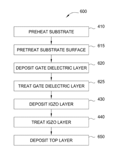
- The use of chemical vapor deposition (CVD) processes for forming IGZO active layers without a prior nucleation layer, combined with in-situ substrate cleaning and preheating, allows for the deposition of high-mobility IGZO layers with controlled stoichiometry and reduced exposure to air, improving throughput and reducing environmental degradation.

Environmental Impact of IGZO Surface Treatment Processes
The environmental implications of IGZO (Indium Gallium Zinc Oxide) surface treatment processes have become increasingly significant as this technology gains wider adoption in display and semiconductor industries. Surface treatments, while critical for enhancing IGZO thin film capabilities, often involve chemicals and processes that pose environmental challenges.
Chemical usage in IGZO surface treatments presents a primary environmental concern. Many conventional treatments utilize fluorine-based compounds, strong acids, and organic solvents that can contribute to air and water pollution if not properly managed. These chemicals may have high global warming potentials, ozone depletion properties, or persistence in the environment. For instance, plasma treatments using CF4 or SF6 gases contribute to greenhouse gas emissions, with global warming potentials thousands of times greater than CO2.
Water consumption represents another significant environmental impact. Wet chemical treatments and cleaning processes require substantial amounts of ultra-pure water, contributing to water scarcity issues in regions where manufacturing facilities operate. Additionally, the wastewater generated contains various contaminants including heavy metals like indium and gallium, which require specialized treatment before discharge.
Energy intensity of surface treatment processes also contributes to their environmental footprint. Plasma treatments, thermal annealing, and vacuum-based processes demand considerable energy inputs, indirectly leading to carbon emissions when powered by non-renewable energy sources. The high-temperature requirements of certain annealing processes further amplify energy consumption.
Recent industry trends show promising developments in green surface treatment technologies. Water-based treatments are gradually replacing solvent-based processes, while dry treatment methods that minimize chemical waste are gaining traction. Some manufacturers have implemented closed-loop systems that recycle treatment chemicals and recover valuable metals from waste streams.
Regulatory frameworks worldwide are increasingly addressing these environmental concerns. The European Union's RoHS and REACH regulations restrict certain hazardous substances used in electronics manufacturing, while similar initiatives in Asia and North America are pushing the industry toward more sustainable practices. These regulations have accelerated research into environmentally benign alternatives for IGZO surface treatments.
Life cycle assessments of IGZO-based devices indicate that improving the environmental profile of surface treatments could significantly reduce the overall ecological footprint of end products. This presents both a challenge and an opportunity for technology developers to balance performance requirements with environmental sustainability in next-generation display and semiconductor technologies.
Manufacturing Scalability of Advanced Surface Treatments
The scalability of advanced surface treatments for IGZO thin films represents a critical factor in transitioning laboratory innovations to commercial manufacturing environments. Current industrial implementation of surface treatments such as plasma processing, chemical passivation, and thermal annealing faces significant challenges when scaled to mass production levels. These challenges primarily stem from maintaining process uniformity across large substrate areas while ensuring consistent film quality and device performance.
Vacuum-based plasma treatments, which have shown excellent results in research settings, require substantial capital investment for large-scale implementation. The cost of high-vacuum equipment increases non-linearly with chamber size, creating economic barriers for manufacturers. Additionally, maintaining plasma uniformity across large substrates (Gen 8 and above) presents technical difficulties that can lead to performance variations across display panels or sensor arrays.
Solution-based surface treatments offer more cost-effective scaling pathways but introduce challenges in chemical waste management and process control. The environmental impact of chemical treatments must be carefully assessed, particularly as production volumes increase. Several manufacturers have developed closed-loop systems that recycle treatment chemicals, reducing both costs and environmental footprint while maintaining treatment efficacy.
Roll-to-roll (R2R) processing represents a promising approach for scaling surface treatments, particularly for flexible IGZO applications. R2R compatible surface treatments have demonstrated throughput rates exceeding 50 m²/min while maintaining acceptable performance metrics. However, the integration of multiple surface treatment steps into continuous R2R lines remains technically challenging, often requiring innovative engineering solutions to maintain process stability.
The semiconductor industry's experience with atomic layer deposition (ALD) provides valuable insights for scaling precise surface treatments. ALD-based passivation layers have shown excellent scalability while providing atomic-level control over interface properties. Several equipment manufacturers have developed specialized tools that can process multiple large substrates simultaneously, significantly improving throughput while maintaining the precision inherent to ALD processes.
Energy consumption represents another critical factor in scaling surface treatments. Thermal annealing processes, while effective for improving IGZO performance, consume substantial energy when implemented at industrial scales. Recent innovations in flash lamp annealing and laser processing offer more energy-efficient alternatives that can be more readily scaled while providing comparable performance benefits. These approaches reduce both operating costs and carbon footprint, aligning with sustainability goals increasingly prioritized by manufacturers.
Unlock deeper insights with Patsnap Eureka Quick Research — get a full tech report to explore trends and direct your research. Try now!
Generate Your Research Report Instantly with AI Agent
Supercharge your innovation with Patsnap Eureka AI Agent Platform!