Research on IGZO Thin Film Cost-Effectiveness for Large Scale Production
SEP 28, 202510 MIN READ
Generate Your Research Report Instantly with AI Agent
Patsnap Eureka helps you evaluate technical feasibility & market potential.
IGZO Technology Background and Production Goals
Indium Gallium Zinc Oxide (IGZO) technology emerged in the early 2000s as a promising semiconductor material for thin-film transistors (TFTs). Initially developed by researchers at Tokyo Institute of Technology and later commercialized by companies like Sharp Corporation, IGZO represents a significant advancement over traditional amorphous silicon (a-Si) and low-temperature polysilicon (LTPS) technologies. The material's unique electron configuration, featuring overlapping s-orbitals of metal cations, enables superior electron mobility—10-20 times higher than a-Si—while maintaining excellent uniformity across large areas.
The evolution of IGZO technology has been driven by increasing demands for higher resolution, lower power consumption, and larger display sizes in consumer electronics. Since its first commercial application in 2012, IGZO has steadily expanded from small mobile displays to large-format panels for televisions and professional monitors, demonstrating its versatility and scalability. Recent advancements have focused on improving stability, reducing defect density, and optimizing deposition techniques to enhance yield rates in mass production environments.
Current technical goals for IGZO thin film production center on achieving cost-effectiveness at scale while maintaining performance advantages. Specifically, the industry aims to reduce material consumption by developing thinner films (sub-50nm) without compromising electrical characteristics. Simultaneously, there is a push to optimize sputtering processes to increase throughput and reduce energy consumption during deposition, as these factors significantly impact overall production costs.
Another critical objective is improving yield rates through better process control and defect management. Current industry standards target defect densities below 0.1 defects/cm², but achieving this consistently across large substrates remains challenging. Enhanced in-line monitoring systems and process automation are being developed to address these challenges and ensure uniform film quality across Gen 10+ substrates (>3m²).
From a sustainability perspective, the industry is working toward reducing the reliance on indium—a relatively scarce element—through alternative material compositions or more efficient utilization. Research into recycling processes for IGZO target materials from production waste represents another avenue for improving long-term cost-effectiveness and environmental sustainability.
The ultimate production goal is to establish IGZO as the dominant TFT technology for next-generation displays by achieving a price point competitive with a-Si while delivering superior performance. This requires balancing material costs, process complexity, and yield rates to reach an optimal cost-performance ratio that enables widespread adoption across multiple product categories, from flexible displays to large-format televisions and transparent electronics.
Market Demand Analysis for IGZO Thin Film Applications
The IGZO (Indium Gallium Zinc Oxide) thin film market is experiencing robust growth driven by increasing demand for high-performance display technologies. The global display market, which serves as the primary application area for IGZO technology, is projected to reach $169 billion by 2025, with IGZO-based displays accounting for a significant portion of this growth. This expansion is primarily fueled by the consumer electronics sector, particularly smartphones, tablets, and large-format televisions, where IGZO's superior electron mobility and transparency characteristics provide substantial advantages.
Consumer electronics manufacturers are increasingly adopting IGZO technology due to its ability to deliver higher resolution displays with lower power consumption. Market research indicates that power efficiency has become a critical purchasing factor for 78% of smartphone consumers, creating strong pull demand for IGZO-based displays. Additionally, the growing trend toward larger screen sizes in both mobile devices and televisions has amplified the need for display technologies that can maintain performance while scaling up in size.
The automotive industry represents an emerging market segment for IGZO applications, with advanced dashboard displays and infotainment systems requiring the high performance and reliability that IGZO can provide. Industry forecasts suggest that automotive display market will grow at a CAGR of 8.5% through 2026, creating new opportunities for IGZO thin film implementation.
Commercial and industrial display applications are also driving demand for IGZO technology. Digital signage, medical imaging displays, and industrial control panels benefit from IGZO's superior refresh rates and image clarity. The healthcare sector in particular has shown increasing interest in IGZO displays for diagnostic imaging equipment, where image quality directly impacts clinical outcomes.
Regional market analysis reveals that East Asia continues to dominate both production and consumption of IGZO-based products, with Japan, South Korea, and Taiwan leading in manufacturing capacity. However, demand is growing rapidly in North American and European markets as consumer awareness of display quality increases and commercial applications expand.
Cost sensitivity varies significantly across market segments. While premium consumer electronics can absorb higher component costs for superior performance, mass-market applications remain highly price-sensitive. Market research indicates that cost reduction is essential for IGZO to penetrate mid-range device segments, where a price premium of no more than 15% over conventional technologies is acceptable to manufacturers.
The market trajectory suggests that as production scales and yields improve, IGZO thin films will continue to displace conventional technologies in an expanding range of applications. However, this transition depends critically on achieving cost-effectiveness in large-scale production to meet price expectations across diverse market segments.
Current Status and Challenges in IGZO Manufacturing
IGZO (Indium Gallium Zinc Oxide) thin film technology has gained significant traction in the display industry over the past decade. Currently, the global manufacturing landscape is dominated by key players in Japan, South Korea, and Taiwan, with emerging capabilities in China. The production technology has matured considerably since its commercial introduction in 2012, yet several challenges persist in achieving optimal cost-effectiveness for large-scale production.
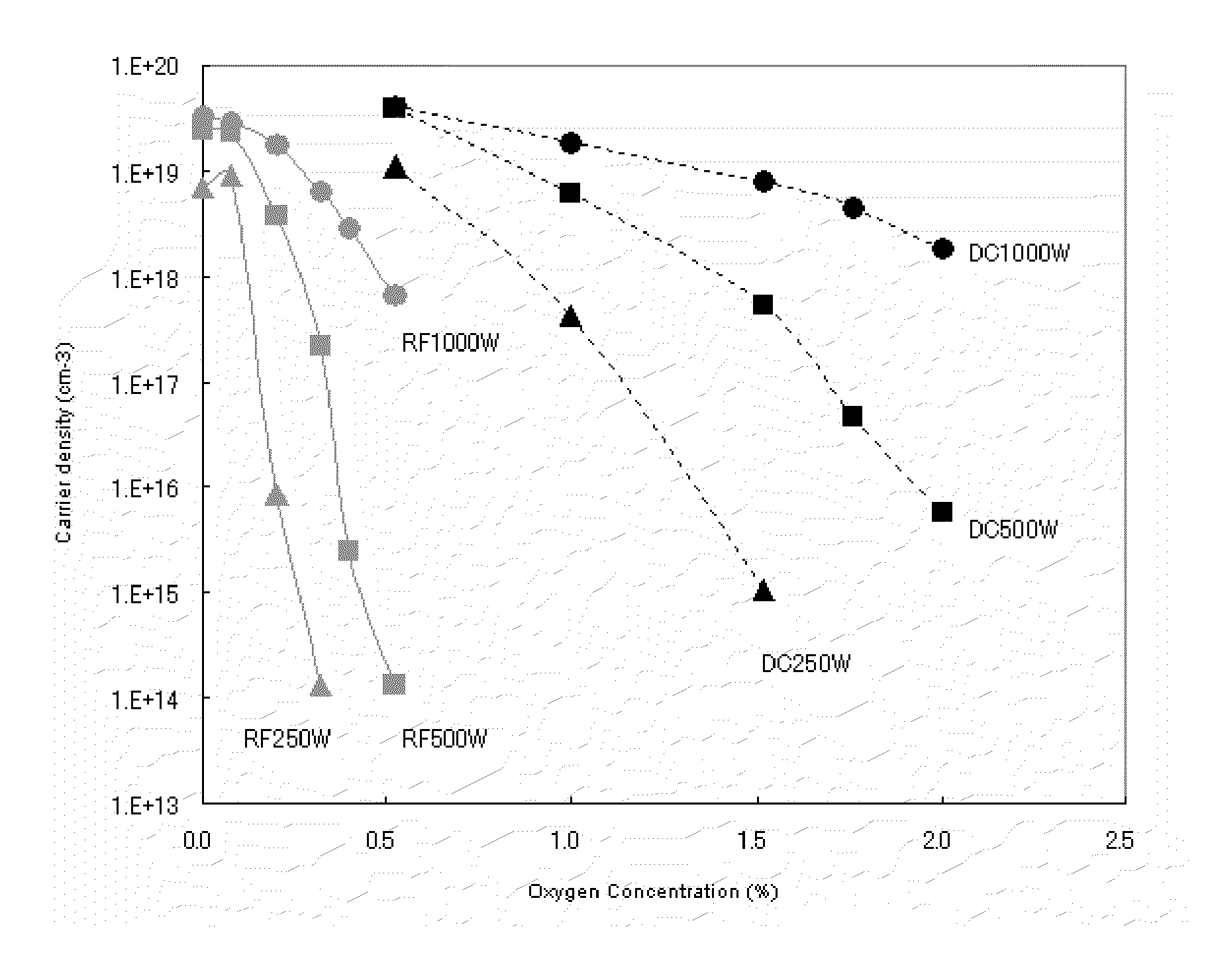
The primary manufacturing methods for IGZO thin films include sputtering deposition, solution processing, and atomic layer deposition (ALD). Among these, RF magnetron sputtering remains the most widely adopted technique in industrial settings due to its reliability and scalability. However, this process faces challenges in material utilization efficiency, with typical utilization rates of indium—a critical and expensive component—hovering around 30-40%.
A significant technical hurdle in IGZO manufacturing is achieving uniform film deposition over large areas while maintaining consistent electrical properties. As display sizes increase beyond 65 inches, maintaining thickness uniformity within ±5% becomes increasingly difficult. This challenge directly impacts production yields, which currently average 80-85% for Gen 8.5 substrates, significantly lower than the 92-95% achieved with conventional a-Si technology.
Material costs represent approximately 40-45% of the total production expenses for IGZO thin films. Indium, being a rare earth element with limited global reserves, poses both supply chain risks and cost volatility. Current market prices for indium fluctuate between $200-300 per kilogram, with projections indicating potential increases as demand grows across various industries including photovoltaics and touch panels.
Energy consumption during the manufacturing process presents another challenge. The annealing process, essential for optimizing IGZO film properties, typically requires temperatures of 300-350°C for 1-2 hours, contributing significantly to production costs. Recent research has focused on lowering these temperature requirements through process optimization and alternative annealing methods such as microwave and laser annealing.
Equipment depreciation and maintenance costs also impact overall manufacturing economics. The specialized deposition systems for IGZO production typically cost between $5-10 million per unit, with annual maintenance expenses averaging 8-12% of the initial investment. The complexity of these systems necessitates highly skilled operators, adding to operational expenses.
Environmental considerations present additional challenges, particularly regarding the disposal of waste materials containing indium and other metals. Regulatory compliance costs are increasing as environmental standards become more stringent globally, with recycling and recovery processes still being economically suboptimal at industrial scales.
Cost-Effective IGZO Manufacturing Solutions
01 Manufacturing process optimization for cost reduction
Various manufacturing techniques have been developed to optimize the production of IGZO thin films while reducing costs. These include improved deposition methods, lower temperature processes, and simplified fabrication steps that maintain high-quality film characteristics. By optimizing the manufacturing process, manufacturers can achieve cost-effective production of IGZO thin films without compromising performance, making them more competitive for commercial applications.- Manufacturing process optimization for cost reduction: Various manufacturing process optimizations can significantly reduce the production costs of IGZO thin films. These include improved deposition techniques, reduced material waste, and streamlined fabrication steps. By optimizing the manufacturing process, manufacturers can achieve higher throughput, lower energy consumption, and reduced production time, all contributing to enhanced cost-effectiveness of IGZO thin films while maintaining their performance characteristics.
- Material composition and doping strategies: Modifying the material composition and implementing strategic doping of IGZO thin films can improve their cost-effectiveness. By adjusting the ratio of indium, gallium, and zinc, or incorporating alternative materials, manufacturers can reduce dependency on expensive raw materials while maintaining or enhancing electrical performance. Specific doping techniques can also improve stability and conductivity, allowing for thinner films that require less material while delivering comparable performance.
- Scalable production techniques for mass manufacturing: Scalable production techniques enable cost-effective mass manufacturing of IGZO thin films. These include roll-to-roll processing, large-area deposition methods, and automated quality control systems. Such approaches reduce per-unit costs through economies of scale while maintaining consistent film quality across large substrates. The development of specialized equipment and processes for high-volume production further enhances the commercial viability of IGZO technology for various applications.
- Alternative fabrication methods and substrates: Alternative fabrication methods and substrate materials can significantly improve the cost-effectiveness of IGZO thin films. Solution-based processing, printing techniques, and low-temperature deposition methods reduce energy consumption and equipment costs compared to traditional vacuum-based processes. Additionally, using flexible or low-cost substrate materials enables new applications while reducing overall production expenses. These approaches maintain the essential electrical properties of IGZO while making the technology more accessible for various market segments.
- Performance optimization for specific applications: Tailoring IGZO thin film properties for specific applications can enhance cost-effectiveness by optimizing performance where it matters most. By adjusting film thickness, annealing conditions, and interface engineering based on application requirements, manufacturers can avoid over-engineering and reduce material usage. This targeted approach ensures that resources are allocated efficiently, with performance characteristics optimized for specific use cases such as displays, sensors, or memory devices, resulting in better cost-performance ratios.
02 Material composition and doping strategies
Innovations in material composition and doping strategies have led to more cost-effective IGZO thin films. By adjusting the ratio of indium, gallium, and zinc, or incorporating alternative dopants, researchers have developed formulations that reduce dependency on expensive raw materials while maintaining or enhancing electrical properties. These approaches help address the cost concerns related to indium, which is one of the more expensive components in IGZO films.Expand Specific Solutions03 Device structure and integration techniques
Innovative device structures and integration techniques have been developed to enhance the cost-effectiveness of IGZO thin film applications. These include simplified transistor architectures, reduced layer counts, and improved interfaces between IGZO and other materials. Such structural optimizations reduce material usage and processing steps, leading to lower manufacturing costs while maintaining device performance in applications such as displays and sensors.Expand Specific Solutions04 Performance enhancement for longer device lifetime
Methods to enhance the stability and performance of IGZO thin films have been developed to extend device lifetime, thereby improving long-term cost-effectiveness. These include passivation techniques, stress reduction methods, and environmental protection strategies that prevent degradation of electrical properties over time. By extending the operational lifetime of IGZO-based devices, the overall cost of ownership is reduced, making these technologies more economically viable despite potentially higher initial production costs.Expand Specific Solutions05 Alternative fabrication equipment and scaling techniques
Development of specialized fabrication equipment and scaling techniques has contributed to more cost-effective production of IGZO thin films. These include modified sputtering systems, solution-based processing methods, and large-area deposition techniques that enable higher throughput and material efficiency. By addressing equipment costs and scaling challenges, these innovations help reduce the overall manufacturing expenses and make IGZO technology more accessible for mass production applications.Expand Specific Solutions
Key Industry Players in IGZO Thin Film Production
The IGZO thin film market is currently in a growth phase, with increasing adoption in large-scale display manufacturing due to its superior electron mobility and transparency compared to traditional materials. The global market size for IGZO technology is expanding rapidly, driven by demand for high-resolution displays in consumer electronics. While technical maturity has advanced significantly, cost-effectiveness for mass production remains challenging. Leading players like Samsung Display, LG Display, and BOE Technology are investing heavily in IGZO manufacturing optimization, while Sharp Corp (an early IGZO pioneer) continues to hold significant intellectual property. Research institutions including Korea Atomic Energy Research Institute and Fudan University are developing next-generation processes to reduce production costs, with ULVAC providing critical manufacturing equipment solutions.
ULVAC INC
Technical Solution: ULVAC has developed specialized equipment and processes for cost-effective IGZO thin film production at industrial scale. Their technology centers around advanced physical vapor deposition (PVD) systems specifically optimized for oxide semiconductor deposition. ULVAC's approach features a proprietary rotary magnet sputtering source that achieves exceptional uniformity (±2.5% across Gen 8+ substrates) while maximizing target utilization to over 75%, significantly reducing material costs[9]. Their systems incorporate precise gas flow control with multiple independent zones that optimize the oxidation state of the deposited film while minimizing oxygen consumption. ULVAC has also developed a unique target bonding technology that improves thermal conductivity and allows for higher power operation without cracking, increasing deposition rates by approximately 30% compared to conventional bonding methods[10]. Additionally, their equipment features an innovative chamber design that reduces contamination and enables faster pump-down times, improving throughput and reducing energy consumption. ULVAC's integrated process monitoring system provides real-time feedback on critical parameters including plasma characteristics, deposition rate, and film properties, enabling tight process control that maximizes yield rates.
Strengths: Industry-leading equipment design specifically optimized for IGZO deposition; excellent target utilization reducing material costs; comprehensive process knowledge covering the entire deposition workflow. Weaknesses: High initial equipment investment cost; requires specialized technical expertise for optimal operation and maintenance; somewhat limited flexibility for rapid process changes compared to smaller research-scale systems.
SAMSUNG DISPLAY CO LTD
Technical Solution: Samsung Display has developed an advanced IGZO thin film fabrication technology specifically engineered for cost-effective large-scale production. Their approach utilizes a modified co-sputtering technique that allows precise control of the In:Ga:Zn ratio (typically 1:1:1 to 2:2:1) to optimize both performance and material costs[5]. Samsung's process incorporates a unique pre-treatment of the substrate surface that improves adhesion and uniformity while reducing defect density. They've implemented a multi-layer deposition strategy where ultra-thin IGZO layers (15-20nm each) are sequentially deposited with controlled intermittent plasma treatments, resulting in superior electrical characteristics while minimizing material consumption. Samsung has also pioneered a rapid thermal processing technique that reduces annealing time by approximately 40% compared to conventional methods[6]. Their manufacturing system integrates real-time monitoring with AI-based process control that automatically adjusts parameters to maintain optimal film quality, significantly improving yield rates to over 95% for large area substrates.
Strengths: Exceptional uniformity across large substrates (up to Gen 10.5); highly automated production system reducing labor costs; excellent stability and reliability of the resulting TFTs with minimal performance degradation over time. Weaknesses: Relatively complex equipment configuration requiring specialized maintenance; higher initial capital investment compared to traditional oxide semiconductor production lines.
Critical Patents and Technical Innovations in IGZO
Method for producing a-IGZO oxide thin film
PatentActiveUS8148245B2
Innovation
- A method involving direct current sputtering with a sintered oxide target of indium, gallium, and zinc, optimized with specific composition ratios and resistance, and subsequent annealing in an oxygen-rich atmosphere to stabilize carrier density, allowing for high reproducibility and suitable for large-area deposition.
Indium gallium zinc oxide, production method and application thereof
PatentActiveJP2014005165A
Innovation
- A method involving the uniform mixing of indium, gallium, and zinc at the atomic level using coprecipitation or ball milling, followed by calcination, to produce a high-quality IGZO target material with uniform particle size and high specific surface area, reducing the formation of second-phase compounds.
Supply Chain Optimization for IGZO Production
The optimization of the IGZO (Indium Gallium Zinc Oxide) supply chain represents a critical factor in achieving cost-effectiveness for large-scale production. Current supply chain structures for IGZO materials face significant challenges, primarily due to the limited availability and geographical concentration of key raw materials, particularly indium, which is classified as a critical material with supply risks.
Material sourcing presents the first major challenge in the IGZO supply chain. Indium, primarily obtained as a by-product of zinc mining, faces potential supply constraints with approximately 70% of global production concentrated in China. Establishing diversified sourcing strategies and developing relationships with multiple suppliers across different regions can mitigate these risks and ensure stable material flow.
Transportation and logistics optimization offers substantial cost-saving opportunities. The sensitive nature of IGZO precursor materials requires specialized handling and transportation conditions. Implementing regional manufacturing hubs closer to end-users can significantly reduce transportation costs and carbon footprint while improving delivery reliability. Advanced inventory management systems utilizing predictive analytics can further optimize stock levels and reduce carrying costs.
Manufacturing process integration represents another critical optimization area. Vertical integration of the supply chain—from raw material processing to thin film deposition—can eliminate intermediaries and reduce overall costs. Co-location of material suppliers and thin film manufacturers enables just-in-time delivery systems, minimizing inventory requirements and associated costs while improving production flexibility.
Quality control standardization across the supply chain is essential for reducing waste and rework. Implementing consistent quality standards from raw material suppliers through to final thin film production can significantly reduce rejection rates. Advanced analytical techniques for incoming material inspection can prevent the introduction of substandard materials into the production process.
Recycling and circular economy principles offer promising opportunities for supply chain sustainability. Developing efficient recovery processes for indium and other valuable materials from production waste and end-of-life products can create secondary material streams, reducing dependence on primary sources. Several manufacturers have already implemented closed-loop recycling systems that recover up to 60% of indium from production waste.
Strategic partnerships and long-term agreements with key suppliers can provide pricing stability and preferential access to materials during supply constraints. Collaborative development initiatives with suppliers can also drive innovation in material formulations and processing techniques, potentially reducing material requirements or enabling substitution of critical components.
Environmental Impact of IGZO Manufacturing Processes
The manufacturing processes of IGZO (Indium Gallium Zinc Oxide) thin films present significant environmental considerations that must be evaluated when scaling production. The primary environmental concerns stem from the extraction and processing of raw materials, particularly indium, which is classified as a critical raw material due to its scarcity and geographically concentrated supply chains. Mining operations for these materials contribute to habitat disruption, soil erosion, and potential water contamination in extraction regions.
During the manufacturing phase, IGZO production typically employs vacuum-based deposition techniques such as sputtering, which consume substantial energy. The energy intensity of these processes contributes to indirect carbon emissions, varying significantly based on the regional energy mix powering production facilities. Facilities operating on renewable energy sources demonstrate markedly lower environmental footprints compared to those dependent on fossil fuels.
Chemical usage in IGZO manufacturing presents another environmental challenge. The etching processes utilize acids and solvents that require careful handling and disposal protocols. While closed-loop systems can recapture and recycle many of these chemicals, residual waste management remains an environmental concern. Advanced facilities have implemented sophisticated filtration and treatment systems to minimize harmful emissions and effluents.
Water consumption represents a substantial environmental factor in IGZO production. The manufacturing process requires ultra-pure water for cleaning substrates and equipment, with production of a single display potentially consuming hundreds of liters. Water recycling technologies have been developed to address this issue, though implementation varies across manufacturing facilities globally.
Comparative lifecycle assessments indicate that IGZO thin films generally offer environmental advantages over alternative semiconductor technologies. The lower processing temperatures of IGZO reduce energy requirements compared to traditional silicon-based semiconductors, while the extended lifespan of IGZO devices potentially reduces electronic waste generation. Additionally, the superior power efficiency of IGZO-based displays contributes to reduced energy consumption during product use phases.
Recent innovations in green manufacturing techniques for IGZO include water-based deposition methods, low-temperature processes, and substitution of hazardous chemicals with environmentally benign alternatives. Several leading manufacturers have established ambitious environmental targets, implementing zero-waste initiatives and carbon neutrality roadmaps for their IGZO production lines.
Regulatory frameworks governing IGZO manufacturing vary significantly by region, with the European Union's RoHS and REACH regulations imposing the most stringent requirements on hazardous substance usage and waste management. As environmental standards continue to evolve globally, manufacturers are increasingly adopting proactive approaches to environmental compliance, recognizing that sustainable production practices represent both an ethical imperative and a competitive advantage in the marketplace.
Unlock deeper insights with Patsnap Eureka Quick Research — get a full tech report to explore trends and direct your research. Try now!
Generate Your Research Report Instantly with AI Agent
Supercharge your innovation with Patsnap Eureka AI Agent Platform!