Analysis of the Role of IGZO Thin Film in Quantum Dot Technology
SEP 28, 20259 MIN READ
Generate Your Research Report Instantly with AI Agent
Patsnap Eureka helps you evaluate technical feasibility & market potential.
IGZO-QD Integration Background and Objectives
The integration of Indium Gallium Zinc Oxide (IGZO) thin films with Quantum Dot (QD) technology represents a significant advancement in display and optoelectronic technologies. This convergence has evolved from separate developmental paths that began in the early 2000s, when IGZO emerged as a promising thin-film transistor (TFT) material and quantum dots gained attention for their unique optical properties. The historical trajectory shows accelerated development after 2010, when researchers recognized the complementary nature of these technologies.
IGZO thin films, characterized by their high electron mobility, transparency, and low processing temperatures, have revolutionized the backplane technology for displays. Concurrently, quantum dots have established themselves as superior color conversion materials, offering narrow emission spectra and tunable bandgaps that enable exceptional color purity and gamut. The integration of these technologies aims to overcome limitations in current display technologies, particularly regarding energy efficiency, color accuracy, and form factor flexibility.
The primary technical objectives of IGZO-QD integration include enhancing electron transport between the IGZO layer and quantum dots, optimizing interface engineering to reduce energy barriers, and developing manufacturing processes compatible with large-scale production. Additionally, researchers are focusing on improving the stability of this hybrid system under various operational conditions, including high brightness levels and extended usage periods.
Market trends indicate growing demand for high-performance displays in consumer electronics, automotive interfaces, and medical imaging, driving research investment in this field. The technology evolution suggests a shift from traditional LCD and OLED technologies toward quantum dot-enhanced displays with advanced backplane technologies like IGZO. This transition is expected to enable next-generation display applications requiring ultra-high resolution, low power consumption, and potentially flexible or transparent form factors.
Current research is exploring multiple integration architectures, including direct deposition of quantum dots onto IGZO substrates, sandwich structures with intermediate transport layers, and novel composite materials combining IGZO and QD properties. Each approach presents distinct advantages and challenges regarding charge transfer efficiency, optical performance, and manufacturing complexity.
The anticipated technological trajectory suggests that IGZO-QD integration will progress toward increasingly sophisticated structures with precisely engineered interfaces, potentially incorporating additional functional materials to enhance performance characteristics. This evolution is expected to enable applications beyond displays, including advanced sensors, photovoltaics, and quantum information processing devices.
Market Analysis for IGZO-Enhanced Quantum Dot Applications
The IGZO-enhanced quantum dot market is experiencing robust growth, driven by increasing demand for high-performance display technologies. The global quantum dot display market, currently valued at approximately 4.5 billion USD, is projected to reach 22 billion USD by 2028, representing a compound annual growth rate of 30.4%. Within this expanding market, IGZO thin film technology is carving out a significant niche due to its superior electron mobility and transparency characteristics when combined with quantum dot materials.
Consumer electronics represents the largest application segment, accounting for nearly 65% of the IGZO-enhanced quantum dot market. This dominance is primarily attributed to the technology's implementation in premium televisions, smartphones, and tablets where manufacturers seek to differentiate their products through superior display quality. Samsung and LG Display have emerged as market leaders, collectively holding approximately 48% market share in IGZO-quantum dot display technologies.
The healthcare and medical imaging sector is emerging as the fastest-growing application segment, with a projected growth rate of 36.2% through 2027. The exceptional color accuracy and energy efficiency of IGZO-quantum dot combinations make them particularly valuable for diagnostic imaging equipment where precision is paramount.
Geographically, East Asia dominates the production landscape, with South Korea, Japan, and Taiwan accounting for over 70% of global manufacturing capacity. However, North America and Europe represent the largest consumer markets, collectively accounting for approximately 58% of global revenue generation.
Market penetration analysis reveals significant untapped potential in automotive displays, where IGZO-quantum dot technology could revolutionize dashboard and entertainment systems. This segment is expected to grow at 34.8% annually as automotive manufacturers increasingly adopt advanced display technologies in mid-range and premium vehicles.
Price sensitivity remains a critical market factor, with current manufacturing costs approximately 30% higher than conventional display technologies. However, economies of scale and manufacturing innovations are expected to reduce this premium to under 15% by 2025, potentially accelerating market adoption across more price-sensitive segments.
The competitive landscape is characterized by strategic partnerships between quantum dot material developers and display manufacturers, with over 40 significant collaboration agreements announced in the past three years. These partnerships aim to optimize the integration of IGZO thin films with quantum dot materials to maximize performance while reducing production costs.
IGZO Thin Film Technology: Current Status and Challenges
Indium Gallium Zinc Oxide (IGZO) thin film technology has emerged as a significant advancement in semiconductor materials, particularly for display technologies and, more recently, in quantum dot applications. Currently, IGZO thin films are predominantly manufactured using physical vapor deposition methods, with sputtering being the most widely adopted industrial technique due to its scalability and cost-effectiveness. The global market has seen substantial adoption of IGZO in TFT backplanes for high-resolution displays, with major production facilities concentrated in East Asia, particularly Japan, South Korea, and Taiwan.
Despite its commercial success, IGZO thin film technology faces several critical challenges. The most pressing technical limitation is the trade-off between carrier mobility and stability. While IGZO offers mobility values typically ranging from 10-15 cm²/Vs—significantly higher than amorphous silicon—this remains insufficient for next-generation quantum dot applications that require faster electron transport. Additionally, the performance of IGZO films exhibits high sensitivity to oxygen partial pressure during deposition, creating manufacturing consistency challenges across large substrates.
Another significant challenge is the degradation of IGZO properties under prolonged bias stress and illumination, particularly problematic for quantum dot integration where light exposure is inherent to the application. This phenomenon, known as negative bias illumination stress (NBIS), causes threshold voltage shifts that compromise device reliability over time. Research efforts are currently focused on passivation techniques and compositional modifications to mitigate these effects.
From a manufacturing perspective, achieving uniform deposition across increasingly larger substrates presents considerable difficulties. As display manufacturers push toward Gen 10.5 and larger fabrication facilities, maintaining consistent IGZO properties becomes exponentially more challenging. The industry is actively exploring advanced process control systems and alternative deposition techniques to address this scaling issue.
When specifically considering quantum dot technology integration, IGZO faces unique challenges related to interface engineering. The electronic band alignment between IGZO and various quantum dot materials requires precise control to facilitate efficient charge transfer while minimizing interfacial defects. Current research indicates that surface modification of either the IGZO layer or the quantum dots is necessary to optimize this critical interface.
Environmental stability represents another obstacle, as IGZO films can be sensitive to ambient conditions, particularly humidity. This necessitates effective encapsulation strategies, especially critical for quantum dot applications where environmental degradation can significantly impact optical and electronic performance. Recent developments in atomic layer deposition (ALD) barrier films show promise for addressing this vulnerability.
Current Technical Solutions for IGZO-QD Integration
01 IGZO thin film transistors for quantum dot displays
Indium Gallium Zinc Oxide (IGZO) thin film transistors are used as backplane technology for quantum dot displays due to their high electron mobility, transparency, and low power consumption. These transistors provide stable current to drive quantum dot pixels, resulting in improved display performance with higher resolution and better color accuracy. The amorphous structure of IGZO allows for uniform electrical characteristics across large areas, making it ideal for quantum dot display applications.- IGZO thin film transistors for quantum dot displays: Indium Gallium Zinc Oxide (IGZO) thin film transistors are used as backplane technology for quantum dot displays due to their high electron mobility, transparency, and low power consumption. These transistors provide stable current to drive quantum dot pixels, resulting in improved display performance with higher resolution, faster response times, and better color accuracy. The amorphous structure of IGZO allows for uniform electrical characteristics across large display areas.
- Quantum dot integration with IGZO semiconductor layers: Quantum dots can be integrated with IGZO semiconductor layers to create advanced optoelectronic devices. This integration combines the excellent charge transport properties of IGZO with the tunable optical properties of quantum dots. Various deposition techniques are used to create multilayer structures where quantum dots are either embedded within or placed adjacent to IGZO layers. This configuration enhances light emission efficiency, photodetection capabilities, and enables novel sensing applications.
- IGZO thin film fabrication methods for quantum dot applications: Specialized fabrication methods are employed to create IGZO thin films compatible with quantum dot technology. These include sputtering, solution processing, and atomic layer deposition techniques optimized for low temperature processing to preserve quantum dot properties. Post-deposition treatments such as annealing in controlled atmospheres help optimize the electrical characteristics of IGZO while maintaining compatibility with quantum dot materials. These methods enable the creation of flexible, transparent devices with high performance characteristics.
- Hybrid IGZO-quantum dot photodetectors and sensors: Hybrid structures combining IGZO thin films with quantum dots create highly sensitive photodetectors and sensors. The quantum dots absorb light at specific wavelengths determined by their size and composition, generating electron-hole pairs that are efficiently collected by the IGZO layer. This configuration enables photodetection across a wide spectral range from ultraviolet to infrared. The high carrier mobility of IGZO enhances response speed while quantum dots provide wavelength selectivity, making these hybrid devices suitable for imaging, environmental monitoring, and biomedical sensing applications.
- IGZO passivation and interface engineering for quantum dot devices: Interface engineering and passivation techniques are critical for optimizing IGZO thin film performance in quantum dot devices. Various dielectric materials and surface treatments are used to reduce trap states at the IGZO-quantum dot interface, improving charge transfer efficiency and device stability. Passivation layers protect both IGZO and quantum dots from environmental degradation while maintaining electrical connectivity between the components. These techniques extend device lifetime, enhance quantum efficiency, and improve operational stability under various environmental conditions.
02 Fabrication methods of IGZO thin films for quantum dot integration
Various deposition techniques are employed to fabricate IGZO thin films for quantum dot technology, including sputtering, atomic layer deposition, and solution processing. These methods control the composition, thickness, and crystallinity of IGZO films, which directly affect their electrical properties. Post-deposition treatments such as annealing in different atmospheres optimize the performance of IGZO films by reducing defects and improving carrier mobility, which is crucial for quantum dot device operation.Expand Specific Solutions03 IGZO-quantum dot hybrid structures for optoelectronic applications
Hybrid structures combining IGZO thin films with quantum dots create advanced optoelectronic devices with enhanced functionality. These structures leverage the excellent charge transport properties of IGZO and the tunable optical properties of quantum dots. The integration enables novel applications such as photodetectors, image sensors, and light-emitting devices with improved efficiency and spectral response. The interface engineering between IGZO and quantum dots is critical for optimizing charge transfer and device performance.Expand Specific Solutions04 IGZO thin film characteristics for quantum dot device performance
The electrical and optical properties of IGZO thin films significantly impact quantum dot device performance. Key characteristics include carrier concentration, mobility, band gap, and transparency, which can be tuned by adjusting the composition ratio of indium, gallium, and zinc. The stability of IGZO under various environmental conditions affects the long-term reliability of quantum dot devices. Optimizing these properties enables better charge injection and extraction in quantum dot layers, resulting in more efficient and stable devices.Expand Specific Solutions05 Novel device architectures combining IGZO and quantum dots
Innovative device architectures that integrate IGZO thin films with quantum dots enable next-generation display and sensing technologies. These include vertically stacked structures, lateral heterojunctions, and patterned arrays that optimize the interaction between IGZO and quantum dots. Such architectures facilitate enhanced charge transport, improved light extraction or absorption, and better device scalability. Advanced manufacturing techniques allow for precise control over the spatial arrangement of IGZO and quantum dot layers, enabling devices with superior performance characteristics.Expand Specific Solutions
Key Industry Players in IGZO-QD Development
The IGZO thin film technology in quantum dot displays is currently in a growth phase, with the market expanding rapidly due to increasing demand for high-resolution, energy-efficient displays. The global market is projected to grow significantly as major players like Samsung Display, BOE Technology, and Sharp Corp. advance their technological capabilities. These companies are investing heavily in R&D to overcome challenges in mass production and stability. ULVAC, TCL, and AGC are developing specialized manufacturing equipment and materials, while research institutions like South China University of Technology and Southeast University are contributing fundamental innovations. The technology is approaching commercial maturity, with leading manufacturers transitioning from research to production phases, though further refinements in manufacturing processes and cost reduction remain priorities.
SAMSUNG DISPLAY CO LTD
Technical Solution: Samsung Display has developed advanced IGZO-QD hybrid display technology that combines the benefits of IGZO thin film transistors with quantum dot color conversion layers. Their approach involves using IGZO as both the active semiconductor layer in TFTs and as a charge transport layer that interfaces with quantum dot materials. The company has created a specialized deposition process that achieves IGZO films with exceptionally low defect density (<10^16 cm^-3) and high uniformity (thickness variation <3%). This enables more precise control of electron flow to quantum dot layers, resulting in superior color purity and brightness stability. Samsung Display's technology incorporates a unique passivation technique that protects IGZO from environmental degradation while maintaining optimal electrical contact with quantum dot materials. Their latest implementations achieve brightness levels exceeding 1,500 nits while maintaining power efficiency, with IGZO's wide bandgap (approximately 3.5 eV) contributing to reduced leakage current and improved display contrast ratios.
Strengths: Exceptional color accuracy and brightness stability; reduced power consumption; excellent scalability for various display sizes; compatibility with next-generation display architectures. Weaknesses: Complex manufacturing process requiring tight quality control; higher initial production costs; requires specialized expertise in both IGZO and quantum dot materials engineering.
BOE Technology Group Co., Ltd.
Technical Solution: BOE has developed a comprehensive IGZO-quantum dot integration platform focused on large-format display applications. Their approach utilizes IGZO thin films with precisely controlled oxygen vacancy concentrations to optimize carrier mobility (achieving 15-20 cm²/Vs) while maintaining excellent stability. BOE's technology incorporates a multi-layer IGZO structure with varying compositions to create an optimal interface with quantum dot materials, enhancing electron injection efficiency and color performance. The company has pioneered a low-temperature IGZO deposition process (below 250°C) specifically designed for quantum dot compatibility, preventing thermal degradation of quantum dot materials during manufacturing. Their solution includes proprietary surface treatment techniques that improve the adhesion between IGZO and quantum dot layers while minimizing interfacial defects. BOE has demonstrated displays utilizing this technology with response times below 1ms and power consumption reductions of up to 40% compared to conventional LCD technologies, while maintaining quantum dot color performance with over 95% BT.2020 coverage.
Strengths: Excellent scalability for large-format displays; superior power efficiency; compatibility with various quantum dot materials; high production yield. Weaknesses: Relatively new technology with limited long-term reliability data; higher initial investment costs; requires specialized manufacturing equipment.
Critical Patents and Research on IGZO-QD Interfaces
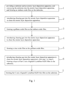
C-axis aligned crystalline IGZO thin film and manufacture method thereof
PatentInactiveUS20190153595A1
Innovation
- A method using atomic layer deposition to form C-axis Aligned Crystalline IGZO thin films by sequentially depositing indium oxide, gallium oxide, and zinc oxide layers on a substrate with controlled temperature, oxygen concentration, and deposition power, resulting in a larger crystalline area with reduced oxygen defects.
Gallium precursors for deposition of gallium-containing oxide films
PatentWO2022266449A1
Innovation
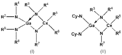
- Development of liquid, non-pyrophoric, halide-free gallium precursors with high vapor pressure, such as (NMe2)2Ga(EtNCH2CH2NMe2), that are thermally stable and compatible with indium and zinc precursors, enabling efficient deposition through vapor deposition processes like ALD and CVD.
Manufacturing Processes and Scalability Considerations
The manufacturing processes for integrating IGZO (Indium Gallium Zinc Oxide) thin films with quantum dot technology present significant challenges and opportunities for commercial scalability. Current production methods primarily utilize physical vapor deposition techniques, with sputtering being the most widely adopted industrial approach due to its ability to create uniform IGZO layers across large substrates. This process typically operates at temperatures between 200-350°C, which must be carefully controlled to prevent degradation of the quantum dot structures.
Solution-based deposition methods are emerging as promising alternatives for cost-effective manufacturing. Techniques such as spin-coating and inkjet printing of IGZO precursors can significantly reduce capital equipment costs compared to vacuum-based systems. However, these methods currently face challenges in achieving the same level of film uniformity and electrical performance as vacuum-deposited films, particularly when scaled to larger dimensions.
Roll-to-roll processing represents a potentially transformative manufacturing approach for IGZO-quantum dot integration. This continuous production method could dramatically increase throughput while reducing costs, but requires further development to address issues of film adhesion and interface quality between the IGZO layer and quantum dot structures. Current roll-to-roll implementations have demonstrated promising results for substrates up to 500mm wide, though defect densities remain higher than those achieved with batch processing.
Material utilization efficiency presents another critical consideration for scalability. Conventional sputtering processes typically achieve material utilization rates of only 30-40%, resulting in significant waste of indium—a relatively scarce and expensive element. Advanced target designs and deposition configurations have shown potential to increase this efficiency to 60-70%, substantially improving the economic viability of large-scale production.
Post-deposition processing steps, including annealing treatments, significantly impact both performance and manufacturing complexity. Optimized rapid thermal annealing protocols have been developed that can reduce processing time from hours to minutes while maintaining or even enhancing electrical properties of the IGZO-quantum dot interface. These advancements are crucial for integration into high-volume manufacturing environments.
Yield management represents perhaps the most significant scalability challenge. Current pilot production lines demonstrate yields of approximately 80-85% for IGZO-integrated quantum dot displays, compared to >95% for conventional display technologies. Automated optical inspection systems combined with machine learning algorithms are being deployed to identify defect patterns and enable process optimization, with recent implementations showing potential to increase yields to the 90-92% range.
Environmental Impact and Sustainability of IGZO-QD Materials
The integration of IGZO (Indium Gallium Zinc Oxide) thin films with quantum dot technology presents significant environmental considerations that warrant thorough examination. The manufacturing processes for both IGZO and quantum dot materials involve potentially hazardous substances, including heavy metals like indium and cadmium, which pose environmental risks if not properly managed. Current production methods typically require substantial energy inputs and generate considerable waste streams, raising concerns about the carbon footprint associated with these advanced materials.
Life cycle assessment studies indicate that IGZO-QD hybrid technologies may offer environmental advantages over conventional display technologies when considering the full product lifecycle. The extended operational lifespan of IGZO-based devices, coupled with their lower power consumption characteristics, contributes to reduced environmental impact during the use phase. However, these benefits must be weighed against the environmental costs of extraction and processing of rare elements required for production.
End-of-life management presents particular challenges for IGZO-QD materials. The complex composition of these hybrid materials complicates recycling efforts, potentially leading to increased e-waste if appropriate recovery systems are not developed. Research into advanced recycling technologies specifically designed for these materials shows promise but remains in early stages of development.
Regulatory frameworks governing the environmental aspects of IGZO-QD materials vary significantly across regions. The European Union's Restriction of Hazardous Substances (RoHS) and Registration, Evaluation, Authorization and Restriction of Chemicals (REACH) regulations impose strict limitations on certain substances used in electronic components, influencing the formulation and production processes for IGZO-QD technologies. Similar regulatory trends are emerging in North America and Asia, though with varying degrees of stringency.
Industry initiatives focused on green chemistry principles are driving innovation toward more sustainable IGZO-QD materials. Recent advancements include the development of cadmium-free quantum dots and water-based processing methods that reduce solvent usage. Additionally, research into bio-inspired quantum dot synthesis shows potential for decreasing the environmental footprint of production processes.
The sustainability profile of IGZO-QD materials is further enhanced by their potential contribution to energy-efficient technologies. Displays incorporating these materials can achieve significant power savings compared to conventional alternatives, potentially offsetting the environmental impact of their production through reduced energy consumption during years of operation. This aspect is particularly relevant in the context of global efforts to reduce carbon emissions and combat climate change.
Unlock deeper insights with Patsnap Eureka Quick Research — get a full tech report to explore trends and direct your research. Try now!
Generate Your Research Report Instantly with AI Agent
Supercharge your innovation with Patsnap Eureka AI Agent Platform!