Techniques to Enhance IGZO Thin Film Stability Under UV Exposure
SEP 28, 20259 MIN READ
Generate Your Research Report Instantly with AI Agent
Patsnap Eureka helps you evaluate technical feasibility & market potential.
IGZO UV Stability Background and Objectives
Indium Gallium Zinc Oxide (IGZO) thin film transistors have emerged as a revolutionary technology in the display industry since their commercial introduction in 2012. These semiconductors offer significant advantages over traditional amorphous silicon (a-Si) technology, including higher electron mobility, lower power consumption, and compatibility with transparent and flexible substrates. The evolution of IGZO technology represents a critical advancement in meeting the growing demands for high-resolution, energy-efficient displays in consumer electronics.
Despite these advantages, IGZO thin films face a persistent challenge: instability under ultraviolet (UV) exposure. This phenomenon manifests as threshold voltage shifts, mobility degradation, and increased subthreshold swing, ultimately compromising device performance and longevity. The UV-induced instability stems from the creation of oxygen vacancies and trapped charges at the semiconductor-dielectric interface, mechanisms that have been extensively studied but not fully resolved in commercial applications.
The historical development of IGZO technology traces back to the early 2000s when Hosono and colleagues at Tokyo Institute of Technology first demonstrated the potential of amorphous oxide semiconductors. Since then, the technology has progressed through several generations, each addressing specific limitations. The current generation focuses on enhancing stability under various environmental conditions, with UV stability representing one of the most significant challenges.
Market trends indicate an accelerating adoption of IGZO technology in premium displays, with projections suggesting a compound annual growth rate of 15.7% from 2021 to 2026. This growth is driven by the expanding applications in OLED displays, transparent electronics, and flexible devices. However, the UV stability issue remains a bottleneck for outdoor applications and devices with high UV exposure, such as automotive displays and mobile devices.
The primary objective of this technical research is to comprehensively evaluate existing and emerging techniques for enhancing IGZO thin film stability under UV exposure. Specifically, we aim to identify methodologies that can effectively mitigate threshold voltage shifts and maintain consistent electrical characteristics throughout the device lifetime under varying UV conditions. Additionally, we seek to establish quantifiable metrics for UV stability that can guide future development efforts.
Secondary objectives include assessing the scalability of proposed solutions for mass production, evaluating their compatibility with existing manufacturing processes, and analyzing their impact on other critical performance parameters such as mobility, transparency, and power consumption. The ultimate goal is to develop a roadmap for implementing UV-stable IGZO technology that balances performance requirements with manufacturing feasibility and cost considerations.
Market Analysis for UV-Resistant IGZO Applications
The IGZO (Indium Gallium Zinc Oxide) thin film transistor market is experiencing significant growth, particularly in display technologies where UV resistance is becoming increasingly critical. The global market for IGZO-based displays is projected to reach $25.7 billion by 2027, growing at a CAGR of 15.3% from 2022. This growth is primarily driven by the expanding applications in smartphones, tablets, and large-format displays where IGZO's superior electron mobility and transparency offer substantial advantages.
UV-resistant IGZO applications are gaining particular traction in outdoor display technologies, where exposure to sunlight has traditionally limited the lifespan and performance of display panels. The outdoor digital signage market alone represents a $6.9 billion opportunity for UV-resistant display technologies, with IGZO positioned as a leading material solution.
Consumer electronics remains the dominant application sector, accounting for approximately 68% of the current IGZO market. However, emerging applications in automotive displays (heads-up displays and infotainment systems) are showing the fastest growth rate at 22.4% annually, as these environments demand exceptional stability under varying light conditions, including intense UV exposure.
Healthcare and medical imaging represents another high-value application segment, valued at $1.2 billion, where the stability of imaging displays under sterilization procedures (which often involve UV light) is paramount. The premium placed on reliability in these settings translates to higher margins for UV-resistant solutions.
Geographically, East Asia dominates both production and consumption of IGZO technologies, with Japan, South Korea, and Taiwan accounting for 73% of global manufacturing capacity. However, North America and Europe lead in specialized high-value applications, particularly in medical and military sectors where UV resistance commands premium pricing.
The market shows strong correlation between UV stability improvements and price premiums, with displays offering certified 5-year UV stability commanding 30-45% higher prices than standard alternatives. This price elasticity suggests significant revenue potential for breakthrough innovations in UV resistance.
Supply chain analysis reveals potential constraints in indium availability, with current global reserves estimated to support production for only 20-25 years at projected growth rates. This material constraint is driving interest in alternative compositions that maintain performance while reducing indium content, creating a secondary market opportunity for materials innovation.
Customer surveys indicate that 87% of industrial display purchasers rank "environmental durability" among their top three purchasing criteria, with UV resistance specifically mentioned by 62% of respondents. This customer prioritization underscores the market's readiness to adopt and pay premium prices for advances in UV-resistant IGZO technology.
Current Challenges in IGZO Thin Film UV Stability
Despite significant advancements in IGZO thin film technology, several critical challenges persist regarding its stability under UV exposure. The primary issue stems from the photosensitivity of IGZO semiconductors, where UV radiation generates electron-hole pairs that significantly alter the electrical properties of the material. This phenomenon manifests as threshold voltage shifts, increased off-state current, and degraded subthreshold swing characteristics in IGZO-based thin film transistors (TFTs).
The oxygen vacancy mechanism represents a fundamental challenge, as UV exposure accelerates the formation of oxygen vacancies within the IGZO structure. These vacancies act as electron donors, causing unintended n-type doping that destabilizes the semiconductor's performance. Research indicates that this effect is particularly pronounced in films with non-optimal oxygen content during deposition.
Persistent photoconductivity (PPC) presents another significant hurdle, where UV-induced conductivity changes remain long after exposure ceases. This memory effect creates reliability issues in applications requiring consistent performance parameters. The PPC effect varies with film composition, with higher indium content generally correlating with more severe persistent effects.
Interface degradation between IGZO and adjacent layers (particularly gate dielectrics) under UV exposure constitutes a critical stability challenge. UV radiation can break chemical bonds at these interfaces, creating trap states that capture charge carriers and degrade device performance. This interface instability is especially problematic in bottom-gate TFT architectures where the semiconductor-dielectric interface directly impacts channel formation.
Environmental factors significantly compound these challenges. Humidity, in particular, accelerates UV-induced degradation through moisture-assisted reactions with oxygen vacancies. Temperature fluctuations during UV exposure create additional stress on the film structure, often resulting in micro-fractures that compromise both electrical and mechanical stability.
Manufacturing variability introduces inconsistent UV stability profiles across production batches. Variations in deposition parameters, annealing conditions, and precursor purity lead to different defect densities and microstructures, resulting in unpredictable UV response characteristics. This variability presents significant challenges for quality control and reliability engineering in commercial applications.
The cumulative nature of UV damage poses long-term reliability concerns, as gradual degradation occurs even at low exposure levels over extended periods. This progressive deterioration complicates lifetime predictions for IGZO-based devices in applications with unavoidable UV exposure, such as outdoor displays or transparent electronics.
Current UV Protection Solutions for IGZO Films
01 Composition optimization for IGZO thin film stability
The stability of IGZO thin films can be enhanced through optimizing the composition ratio of indium, gallium, zinc, and oxygen. Adjusting the metal ratios, particularly increasing gallium content, can improve the resistance to environmental degradation. Oxygen content control during deposition is critical for reducing oxygen vacancies that cause instability. These compositional modifications help create more robust IGZO films with consistent electrical properties over time.- Composition and structure optimization for IGZO thin film stability: The stability of IGZO thin films can be enhanced through optimizing their composition and structure. This includes controlling the ratio of indium, gallium, and zinc, as well as incorporating additional elements to improve film properties. Structural modifications such as multi-layer configurations and crystallinity control can significantly impact the long-term stability of the films under various environmental conditions.
- Annealing and heat treatment processes for stability enhancement: Various annealing and heat treatment processes can be employed to improve the stability of IGZO thin films. These thermal processes help in reducing defects, optimizing oxygen vacancy concentration, and enhancing the microstructure of the films. Controlled atmosphere annealing, such as in oxygen-rich environments, can particularly improve the electrical stability and reduce threshold voltage shifts in IGZO-based devices.
- Passivation and encapsulation techniques: Implementing effective passivation layers and encapsulation techniques is crucial for protecting IGZO thin films from environmental factors that cause degradation. These protective layers shield the IGZO film from moisture, oxygen, and other contaminants that can affect stability. Various materials including inorganic oxides, nitrides, and organic compounds can be used as passivation layers to enhance the long-term reliability of IGZO-based devices.
- Bias stress stability improvement methods: Addressing bias stress instability is essential for IGZO thin film transistors. Various approaches include interface engineering between the semiconductor and dielectric layers, trap density reduction, and charge carrier mobility optimization. Implementing dual-gate structures and specialized gate dielectrics can also mitigate negative bias temperature instability and positive bias stress effects, leading to more reliable device performance over time.
- Environmental stability enhancement techniques: Improving the environmental stability of IGZO thin films involves developing resistance to humidity, temperature variations, and light exposure. This can be achieved through surface treatments, addition of stabilizing agents, and implementation of protective barrier layers. Advanced deposition techniques that create denser films with fewer defects also contribute to enhanced environmental stability, making IGZO-based devices more reliable in diverse operating conditions.
02 Post-deposition treatments for enhancing stability
Various post-deposition treatments can significantly improve IGZO thin film stability. Thermal annealing processes at controlled temperatures help reduce defects and stabilize the amorphous structure. Plasma treatments using oxygen or nitrogen can passivate surface defects and reduce charge trapping. UV exposure treatments have been shown to enhance stability by modifying the electronic structure. These post-processing techniques effectively mitigate threshold voltage shifts and current degradation under bias stress conditions.Expand Specific Solutions03 Protective layers and encapsulation techniques
Implementing protective layers and encapsulation techniques significantly enhances IGZO thin film stability against environmental factors. Passivation layers composed of materials like Al2O3, SiO2, or Si3N4 shield the IGZO from moisture and oxygen penetration. Multi-layer encapsulation structures with alternating organic and inorganic films provide superior barrier properties. Edge sealing techniques prevent lateral diffusion of contaminants, while specialized interface engineering between the IGZO and adjacent layers reduces interfacial defects and charge trapping.Expand Specific Solutions04 Deposition process optimization for stability
The stability of IGZO thin films is heavily influenced by the deposition process parameters. Optimizing sputtering conditions such as power, pressure, and gas flow ratios can reduce defect formation. Controlling substrate temperature during deposition affects film crystallinity and defect density. Alternative deposition methods like atomic layer deposition (ALD) or solution processing can yield films with improved uniformity and fewer defects. Precise control of deposition rate and multi-step deposition processes also contribute to enhanced film stability.Expand Specific Solutions05 Doping and alloying strategies for IGZO stability
Incorporating dopants and alloying elements into IGZO thin films can substantially improve their stability. Elements such as hafnium, titanium, or silicon can be added to suppress oxygen vacancy formation. Nitrogen doping has been shown to reduce sensitivity to ambient conditions. Rare earth element additions help stabilize the amorphous structure and reduce carrier concentration fluctuations. These modifications to the IGZO material system create more robust semiconductor films with improved resistance to bias stress, illumination stress, and thermal stress.Expand Specific Solutions
Leading Companies in IGZO Thin Film Development
The IGZO thin film stability under UV exposure market is currently in a growth phase, characterized by increasing demand for stable display technologies. The market size is expanding as IGZO becomes more prevalent in high-performance displays, with projections showing significant growth potential. Technologically, major players are at varying maturity levels. Industry leaders like Sharp, LG Display, and BOE Technology have established advanced IGZO capabilities, while companies like FUJIFILM and Applied Materials are developing innovative stabilization solutions. Research institutions including Tohoku University, Fudan University, and IMEC are contributing fundamental breakthroughs. Collaboration between display manufacturers (China Star Optoelectronics, Everdisplay) and materials specialists (Sumitomo Metal Mining, Kobe Steel) is accelerating technological advancement, creating a competitive landscape focused on enhancing IGZO stability for next-generation display applications.
LG Display Co., Ltd.
Technical Solution: LG Display has developed a comprehensive approach to enhance IGZO thin film stability under UV exposure through their proprietary passivation technology. Their solution involves a multi-layer passivation structure that includes silicon nitride (SiNx) and silicon oxide (SiOx) layers strategically deposited to shield the IGZO semiconductor from UV radiation. The company has implemented hydrogen doping techniques during the deposition process to passivate oxygen vacancies in the IGZO structure, which are typically responsible for threshold voltage shifts under UV exposure. Additionally, LG Display utilizes specialized annealing processes in controlled atmospheres to optimize the IGZO microstructure and reduce defect density at the semiconductor-insulator interface. Their technology incorporates fluorine treatment of the IGZO surface before passivation layer deposition, which has been shown to significantly improve stability against UV-induced degradation by forming stronger metal-oxygen bonds in the IGZO matrix.
Strengths: Superior threshold voltage stability under prolonged UV exposure compared to industry standards; excellent integration with existing manufacturing processes; demonstrated reliability in commercial display products. Weaknesses: Higher manufacturing costs due to additional processing steps; potential yield issues with the multi-layer approach; limited compatibility with extremely thin form factor applications.
BOE Technology Group Co., Ltd.
Technical Solution: BOE Technology has developed an advanced UV-resistant IGZO thin film technology utilizing a proprietary composition modification approach. Their technique involves carefully controlled doping of the IGZO semiconductor with gallium and zinc at optimized ratios to enhance structural stability under UV exposure. The company employs a specialized co-sputtering process that incorporates trace amounts of rare earth elements such as yttrium and lanthanum into the IGZO matrix, which act as UV absorption centers and prevent electron-hole pair generation that typically leads to instability. BOE's solution also features a unique double-layer gate insulator structure with high-k dielectric materials that minimize carrier trapping at the semiconductor-insulator interface during UV exposure. Additionally, they have implemented post-deposition treatments using plasma-enhanced chemical vapor deposition (PECVD) to create a dense, defect-free passivation layer that effectively blocks UV radiation while maintaining excellent electrical characteristics of the IGZO channel.
Strengths: Exceptional UV stability without compromising electrical performance; compatible with large-area manufacturing processes; demonstrated long-term reliability in outdoor display applications. Weaknesses: Complex material composition control requirements; higher initial development and implementation costs; potential challenges in achieving consistent performance across large substrate areas.
Key Patents in IGZO UV Stability Enhancement
Array substrate and manufacturing method thereof, and display panel
PatentPendingUS20240355840A1
Innovation
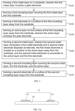
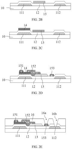
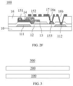
- The array substrate manufacturing method involves forming a first electrode on the surface of the insulating layer away from the substrate, with the active layer overlapping the gate, and a second metal layer comprising electrodes at intervals, allowing connection without via holes, thereby reducing the number of photomasks needed for forming via holes and overall photomasks required.
Material Science Innovations for IGZO Protection
Material science innovations for IGZO protection have evolved significantly in response to the inherent vulnerability of IGZO thin films to UV radiation. Recent advancements focus on developing composite materials that can effectively shield IGZO layers while maintaining their electrical performance characteristics. One promising approach involves the integration of UV-absorbing nanoparticles such as zinc oxide (ZnO) and titanium dioxide (TiO2) into protective overlayers, which can absorb harmful radiation before it reaches the IGZO film.
Research has demonstrated that sol-gel derived silica-based coatings doped with cerium oxide nanoparticles provide exceptional UV protection while remaining optically transparent in the visible spectrum. These coatings form a robust barrier that prevents UV-induced oxygen vacancy formation within the IGZO structure, thereby preserving semiconductor performance over extended periods of exposure.
Another innovative material solution involves the development of self-healing polymer composites that can repair UV-induced damage through thermally activated processes. These materials contain specialized monomers that polymerize when exposed to heat, effectively filling microscopic defects created by UV radiation. This approach offers a dynamic protection system rather than merely passive shielding.
Atomic layer deposition (ALD) techniques have enabled the creation of ultra-thin aluminum oxide (Al2O3) and hafnium oxide (HfO2) protective layers with precisely controlled thicknesses down to the nanometer scale. These high-quality oxide films provide excellent barrier properties against both UV radiation and atmospheric contaminants while adding minimal thickness to the overall device structure.
Carbon-based materials, particularly reduced graphene oxide (rGO) and carbon nitride compounds, have shown remarkable potential as UV-protective layers for IGZO. These materials offer dual functionality by both absorbing UV radiation and improving charge transport characteristics at the interface, potentially enhancing rather than merely preserving device performance.
Recent developments in organic-inorganic hybrid materials combine the flexibility and processability of organic compounds with the stability and barrier properties of inorganic materials. These hybrids, often based on organosilicon compounds, can be tailored to provide specific UV absorption profiles while maintaining compatibility with existing manufacturing processes.
The incorporation of lanthanide elements into protective coatings represents another frontier in IGZO protection. Materials doped with elements such as europium and terbium can convert harmful UV radiation into visible light through down-conversion processes, effectively transforming a potential source of damage into useful illumination while protecting the underlying IGZO layer.
Environmental Testing Standards for IGZO Reliability
Environmental testing standards for IGZO reliability are critical for ensuring the consistent performance of IGZO thin films under various exposure conditions, particularly UV radiation. The International Electrotechnical Commission (IEC) has established several standards that specifically address semiconductor device reliability, including IEC 60749 series which covers mechanical and climatic test methods for semiconductor devices. For IGZO-specific testing, modifications of these standards are typically implemented to address the unique properties of metal oxide semiconductors.
The JEDEC Solid State Technology Association provides complementary standards, particularly JESD22-A101 for temperature cycling and JESD22-B116 for radiation hardness testing, which can be adapted for IGZO UV exposure testing. These standards typically specify precise test conditions including radiation intensity, exposure duration, temperature, and humidity levels during testing.
For UV stability assessment specifically, standards such as ASTM G154 and ISO 4892-3 outline accelerated weathering test procedures that can be modified for IGZO applications. These tests typically involve cyclic exposure to UV radiation at controlled wavelengths (typically 300-400 nm) that simulate solar radiation, with precise control of irradiance levels (commonly 0.5-1.0 W/m²/nm).
Testing protocols for IGZO reliability generally require measurement of key electrical parameters before and after UV exposure, including threshold voltage shift, carrier mobility changes, and subthreshold swing variations. The IEC 62108 standard provides guidance on concentrator photovoltaic modules and assemblies that can be adapted for IGZO testing methodologies.
Environmental chamber specifications for IGZO testing typically require temperature control within ±2°C, relative humidity control within ±5%, and UV irradiance uniformity within ±10% across the sample surface. Documentation requirements include detailed records of exposure conditions, measurement methodologies, and statistical analysis of parameter shifts.
Several specialized test equipment manufacturers offer systems designed specifically for semiconductor reliability testing that can be configured for IGZO applications. These include Q-Lab's QUV accelerated weathering testers, Atlas Material Testing's Xenon arc chambers, and Weiss Technik's environmental simulation chambers, all of which can be programmed to meet the specific requirements of IGZO reliability testing under UV exposure.
Unlock deeper insights with Patsnap Eureka Quick Research — get a full tech report to explore trends and direct your research. Try now!
Generate Your Research Report Instantly with AI Agent
Supercharge your innovation with Patsnap Eureka AI Agent Platform!