Research on Environmental Impact of IGZO Thin Film Production
SEP 28, 202510 MIN READ
Generate Your Research Report Instantly with AI Agent
Patsnap Eureka helps you evaluate technical feasibility & market potential.
IGZO Thin Film Technology Background and Objectives
Indium Gallium Zinc Oxide (IGZO) thin film technology represents a significant advancement in semiconductor materials, emerging in the early 2000s as a promising alternative to amorphous silicon (a-Si) and low-temperature polysilicon (LTPS). The technology was first developed by researchers at Tokyo Institute of Technology, led by Professor Hideo Hosono, who demonstrated the unique properties of this transparent amorphous oxide semiconductor in 2004. Since then, IGZO has evolved from laboratory research to commercial applications, particularly in display technologies.
The evolution of IGZO thin film technology has been driven by increasing demands for higher performance, energy-efficient electronic devices. Traditional semiconductor materials faced limitations in electron mobility, transparency, and manufacturing scalability. IGZO emerged as a solution offering 10-50 times higher electron mobility than a-Si, excellent optical transparency, and compatibility with large-area, low-temperature processing techniques.
From a technical perspective, IGZO combines the advantageous properties of its constituent elements: indium provides high electron mobility, gallium enhances stability and reduces oxygen vacancy formation, and zinc contributes to the amorphous structure while maintaining good electrical properties. This unique composition enables IGZO to achieve a balance of performance characteristics unattainable with previous semiconductor materials.
The primary technical objectives in IGZO thin film research focus on several key areas. First, optimizing deposition methods to achieve consistent film quality while minimizing environmental impact remains a critical goal. Current production methods, including sputtering, pulsed laser deposition, and solution processing, each present different environmental considerations regarding energy consumption, material utilization efficiency, and waste generation.
Second, researchers aim to enhance the stability of IGZO films under various environmental conditions, particularly humidity and temperature fluctuations, which can affect device performance and longevity. This includes developing passivation techniques and optimizing film composition to reduce sensitivity to external factors.
Third, scaling production while maintaining quality and reducing environmental footprint presents significant challenges. As IGZO applications expand beyond displays to include sensors, flexible electronics, and transparent circuits, production volumes increase, amplifying potential environmental impacts.
The technology trajectory suggests continued refinement of deposition techniques, exploration of alternative precursor materials, and development of recycling methods for production waste. Recent research has increasingly focused on reducing the reliance on indium, which faces supply constraints as a rare element, by investigating alternative compositions or more efficient utilization methods.
Market Demand Analysis for Eco-friendly Display Technologies
The global display technology market is witnessing a significant shift toward eco-friendly alternatives, driven by increasing environmental regulations and growing consumer awareness. IGZO (Indium Gallium Zinc Oxide) thin film technology has emerged as a promising solution in this landscape, offering substantial energy efficiency improvements compared to conventional amorphous silicon technologies. Market research indicates that the eco-friendly display technology sector is expected to grow at a compound annual growth rate of 15.7% between 2023 and 2028, reaching a market value of $42.5 billion by the end of this period.
Consumer electronics manufacturers are increasingly prioritizing sustainability in their product development strategies, responding to both regulatory pressures and changing consumer preferences. A recent industry survey revealed that 68% of consumers consider environmental impact when purchasing electronic devices, with 42% willing to pay a premium for products with demonstrably lower environmental footprints. This trend is particularly pronounced in high-income markets across North America, Europe, and parts of Asia.
The commercial demand for IGZO-based displays is being driven by multiple factors beyond environmental concerns. The technology's ability to deliver higher resolution, better transparency, and lower power consumption addresses critical needs in mobile devices, large-format displays, and emerging applications like transparent displays and flexible screens. The healthcare, automotive, and aerospace sectors are showing particular interest in IGZO technology due to its reliability and performance characteristics under varying environmental conditions.
Regulatory frameworks are increasingly influencing market dynamics in this sector. The European Union's Restriction of Hazardous Substances (RoHS) directive, along with similar regulations in other regions, is pushing manufacturers to adopt more environmentally sustainable production processes. Countries including Japan, South Korea, and Taiwan have implemented specific incentives for companies developing and manufacturing eco-friendly display technologies, further stimulating market growth.
Supply chain considerations are becoming increasingly important in market development. The limited availability of indium, a critical component in IGZO production, has raised concerns about long-term scalability and price stability. This has prompted research into alternative materials and more efficient production methods that could reduce material requirements while maintaining performance characteristics.
The competitive landscape is evolving rapidly, with traditional display manufacturers investing heavily in eco-friendly technologies to maintain market relevance. Simultaneously, new entrants specializing in sustainable electronics are gaining traction, particularly in niche applications where environmental credentials carry significant weight. Industry partnerships between material suppliers, equipment manufacturers, and end-product companies are becoming more common as the ecosystem matures and stakeholders recognize the need for collaborative approaches to address technical and environmental challenges.
Current Environmental Challenges in IGZO Manufacturing
The production of Indium Gallium Zinc Oxide (IGZO) thin films presents significant environmental challenges that require immediate attention from manufacturers and regulatory bodies. The primary environmental concern stems from the use of rare and toxic elements, particularly indium, which is classified as a critical raw material due to its limited global supply and concentrated production in few countries. The extraction and processing of indium involves energy-intensive mining operations that contribute to habitat destruction, soil degradation, and water pollution in mining regions.
Manufacturing processes for IGZO thin films typically employ vacuum deposition techniques such as sputtering, which consume substantial amounts of energy and utilize various process gases including argon and oxygen. The high energy consumption associated with maintaining vacuum conditions and plasma generation contributes significantly to the carbon footprint of IGZO production facilities, raising concerns about greenhouse gas emissions and climate impact.
Chemical waste management represents another major environmental challenge in IGZO manufacturing. The production process generates hazardous waste materials including spent targets containing indium, gallium, and zinc residues, contaminated cleaning solutions, and etching chemicals. These wastes require specialized handling and disposal procedures to prevent environmental contamination, yet compliance and proper treatment remain inconsistent across different manufacturing regions.
Water usage and contamination issues are particularly problematic in IGZO production. The manufacturing process requires ultra-pure water for cleaning and processing, with a single manufacturing facility potentially consuming millions of gallons annually. Wastewater from these operations often contains metal particulates and chemical compounds that can be difficult to remove through conventional treatment methods, posing risks to aquatic ecosystems if improperly managed.
Air emissions during IGZO production include volatile organic compounds (VOCs), acid gases, and particulate matter containing metal compounds. These emissions can contribute to local air quality degradation and potentially affect the health of workers and surrounding communities if adequate filtration and scrubbing systems are not implemented and maintained properly.
The end-of-life management of IGZO-containing products presents additional environmental challenges. As these materials are incorporated into consumer electronics with relatively short lifecycles, the recovery and recycling of indium and other valuable components remain technically difficult and economically challenging, resulting in significant material loss to landfills and contributing to electronic waste problems globally.
Regulatory frameworks governing IGZO manufacturing environmental impacts vary significantly across regions, creating inconsistent standards and enforcement. While some jurisdictions have implemented strict regulations on chemical use, emissions, and waste management, others lack comprehensive oversight, potentially creating pollution havens where environmental standards are compromised for economic advantage.
Current Eco-friendly IGZO Production Methods
01 Environmental impact of IGZO thin film manufacturing processes
The manufacturing processes of IGZO (Indium Gallium Zinc Oxide) thin films can have significant environmental impacts. These processes often involve the use of hazardous materials and energy-intensive deposition techniques. Research has focused on developing more environmentally friendly manufacturing methods that reduce waste generation, energy consumption, and the use of toxic substances. Improved processes aim to minimize environmental footprint while maintaining the high performance characteristics of IGZO thin films.- Eco-friendly IGZO thin film manufacturing processes: Various manufacturing processes have been developed to reduce the environmental impact of IGZO thin film production. These include low-temperature deposition methods that consume less energy, solvent-free techniques that minimize chemical waste, and processes that use environmentally benign precursors. These approaches significantly reduce the carbon footprint and hazardous waste generation compared to conventional semiconductor manufacturing.
- Reduced toxic material usage in IGZO fabrication: IGZO thin films can be fabricated with reduced amounts of toxic materials compared to traditional semiconductor materials. Innovations include substituting hazardous chemicals with safer alternatives, minimizing the use of rare earth elements, and developing recycling methods for production waste. These approaches help decrease the environmental burden associated with the extraction and disposal of harmful substances used in electronics manufacturing.
- Energy efficiency improvements in IGZO devices: IGZO thin film transistors offer significant energy efficiency benefits over conventional technologies. Their high electron mobility and low off-state leakage current result in reduced power consumption in electronic devices. This energy efficiency translates to longer battery life in portable devices and lower electricity consumption in displays and other applications, thereby reducing the overall environmental impact during the use phase of products incorporating IGZO technology.
- Recyclability and end-of-life considerations for IGZO components: Research has focused on improving the recyclability of IGZO thin film components at the end of their useful life. Developments include design approaches that facilitate easier separation of materials during recycling, biodegradable substrates for IGZO thin films, and recovery methods for valuable elements from discarded IGZO devices. These innovations help reduce electronic waste and promote a more circular economy in the electronics industry.
- Sustainable applications of IGZO technology: IGZO thin films enable various sustainable applications that can have positive environmental impacts. These include energy-harvesting devices, sensors for environmental monitoring, efficient display technologies that reduce resource consumption, and components for smart grid systems. By enabling these green technologies, IGZO thin films contribute to broader environmental sustainability goals despite the impacts associated with their production.
02 Eco-friendly material composition for IGZO thin films
Innovations in IGZO thin film composition focus on reducing environmental impact through the use of more sustainable materials. This includes developing formulations with lower concentrations of rare or toxic elements, exploring alternative dopants, and creating recyclable or biodegradable components. These eco-friendly compositions aim to maintain or enhance the electrical performance of IGZO while reducing resource depletion and environmental contamination from material extraction and disposal.Expand Specific Solutions03 Energy efficiency and reduced power consumption of IGZO devices
IGZO thin films offer significant environmental benefits through improved energy efficiency in electronic devices. The high electron mobility and low off-state current of IGZO transistors result in reduced power consumption compared to conventional technologies. This energy efficiency translates to longer battery life in portable devices and lower electricity usage in displays and other applications, contributing to reduced carbon emissions over the lifecycle of products incorporating IGZO technology.Expand Specific Solutions04 Recycling and end-of-life management of IGZO thin films
The environmental impact of IGZO thin films at the end of their useful life is an important consideration. Research addresses recycling methods for recovering valuable elements like indium from used IGZO films, reducing the need for new raw material extraction. Techniques for separating IGZO layers from device substrates and other components facilitate more effective recycling. Proper end-of-life management strategies help minimize waste and prevent potential environmental contamination from improper disposal.Expand Specific Solutions05 Sustainable applications and lifecycle assessment of IGZO technology
IGZO thin films enable various sustainable applications that can have positive environmental impacts. These include more efficient displays, sensors for environmental monitoring, and components for renewable energy systems. Lifecycle assessments of IGZO-based devices evaluate their overall environmental footprint from raw material extraction through manufacturing, use, and disposal. These assessments help identify opportunities for improving sustainability throughout the technology lifecycle and demonstrate the net environmental benefits of IGZO compared to alternative technologies.Expand Specific Solutions
Key Industry Players in IGZO Thin Film Market
The IGZO thin film production market is currently in a growth phase, with increasing adoption in display technologies due to superior electron mobility and transparency. The market is expanding rapidly, driven by demand for high-resolution displays in consumer electronics, with projections suggesting a compound annual growth rate of 15-20% over the next five years. Technologically, IGZO has reached commercial maturity but continues to evolve, with companies like Samsung Display, LG Display, and BOE Technology leading innovation. Sharp and ULVAC have established strong intellectual property positions, while Applied Materials and JUSUNG ENGINEERING provide critical manufacturing equipment. Research institutions like Southeast University and Fudan University are advancing next-generation applications, focusing on environmental impact reduction and sustainable production methods.
BOE Technology Group Co., Ltd.
Technical Solution: BOE has pioneered a sustainable IGZO thin film production methodology focused on resource efficiency and pollution reduction. Their process employs room-temperature sputtering techniques that reduce energy requirements by up to 40% compared to conventional thermal processes. BOE has developed proprietary target materials with enhanced durability, extending useful life by approximately 25% and reducing waste generation. Their manufacturing facilities implement advanced water purification and recycling systems that recover and reuse up to 75% of process water. BOE has also implemented innovative gas abatement systems that capture over 90% of potentially harmful emissions from the deposition process. The company utilizes AI-driven process control to optimize material usage, reducing raw material consumption by approximately 15-20%. Additionally, BOE has developed a chemical recovery system that reclaims and purifies solvents used in the cleaning processes, minimizing hazardous waste generation and reducing the environmental footprint of their IGZO production facilities.
Strengths: BOE's approach excels in resource efficiency through innovative target materials and AI-driven process optimization, significantly reducing waste generation while maintaining high production yields. Weaknesses: The complex recycling and abatement systems require substantial maintenance and specialized technical expertise, potentially increasing operational costs and complexity.
SAMSUNG DISPLAY CO LTD
Technical Solution: Samsung Display has developed an eco-friendly IGZO thin film production process that significantly reduces environmental impact compared to conventional methods. Their approach utilizes low-temperature deposition techniques that consume approximately 30% less energy than traditional high-temperature processes. Samsung has implemented a closed-loop water recycling system in their IGZO manufacturing facilities, achieving up to 80% reduction in water consumption. Their process also minimizes the use of toxic precursors by employing alternative, less harmful chemical compounds for indium, gallium, zinc, and oxygen deposition. Samsung has further reduced waste through precise material deposition control systems that optimize target utilization and minimize overspray. The company has also invested in advanced exhaust treatment systems that capture and neutralize potentially harmful emissions before release, reducing air pollutants by approximately 65% compared to industry standards.
Strengths: Samsung's approach significantly reduces energy consumption, water usage, and harmful emissions while maintaining high-quality IGZO film production. Their closed-loop systems represent industry-leading sustainability practices. Weaknesses: The specialized equipment and processes required for their eco-friendly approach increase initial capital costs and may limit production flexibility for certain applications.
Critical Environmental Impact Assessment Studies
Indium gallium zinc oxide, production method and application thereof
PatentActiveJP2014005165A
Innovation
- A method involving the uniform mixing of indium, gallium, and zinc at the atomic level using coprecipitation or ball milling, followed by calcination, to produce a high-quality IGZO target material with uniform particle size and high specific surface area, reducing the formation of second-phase compounds.
C-axis aligned crystalline IGZO thin film and manufacture method thereof
PatentInactiveUS20190153595A1
Innovation
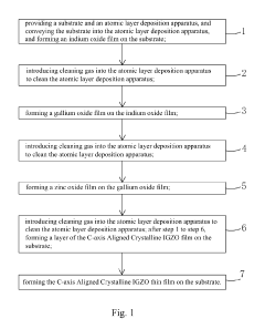
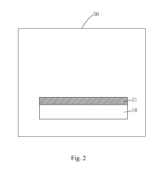
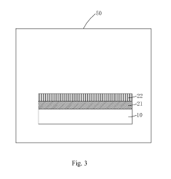
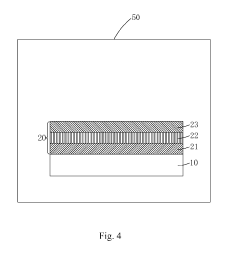
- A method using atomic layer deposition to form C-axis Aligned Crystalline IGZO thin films by sequentially depositing indium oxide, gallium oxide, and zinc oxide layers on a substrate with controlled temperature, oxygen concentration, and deposition power, resulting in a larger crystalline area with reduced oxygen defects.
Regulatory Compliance and Environmental Standards
The production of IGZO (Indium Gallium Zinc Oxide) thin films is subject to increasingly stringent environmental regulations across global jurisdictions. In the United States, the Environmental Protection Agency (EPA) has established specific guidelines under the Clean Air Act and Clean Water Act that govern emissions and waste disposal from semiconductor manufacturing facilities. These regulations mandate strict control of volatile organic compounds (VOCs), hazardous air pollutants, and wastewater containing heavy metals such as indium and gallium.
The European Union enforces even more rigorous standards through the REACH (Registration, Evaluation, Authorization and Restriction of Chemicals) regulation and RoHS (Restriction of Hazardous Substances) directive. IGZO manufacturers operating in EU territories must demonstrate comprehensive chemical safety assessments and implement substitution plans for substances of very high concern (SVHCs). The EU's Industrial Emissions Directive (IED) further requires the application of Best Available Techniques (BAT) for pollution prevention and control.
In Asia, Japan's Ministry of Economy, Trade and Industry (METI) has developed specific environmental guidelines for the electronics manufacturing sector, while China has implemented the Measures for Environmental Management of New Chemical Substances. South Korea's Chemical Control Act similarly imposes strict reporting and management requirements for hazardous substances used in thin film production.
ISO 14001 certification has become a de facto industry standard for IGZO manufacturers, requiring the implementation of effective environmental management systems. Additionally, the Responsible Business Alliance (formerly EICC) Code of Conduct sets forth environmental performance standards that many electronics companies require their suppliers to meet, including IGZO thin film producers.
Emerging regulations are increasingly focusing on circular economy principles, with extended producer responsibility (EPR) schemes requiring manufacturers to consider the entire lifecycle environmental impact of their products. This has led to innovations in IGZO production processes that minimize waste generation and facilitate material recovery and recycling.
Carbon footprint regulations are also becoming more prevalent, with many jurisdictions implementing carbon pricing mechanisms that affect energy-intensive manufacturing processes like IGZO thin film production. Companies are increasingly required to report their greenhouse gas emissions and demonstrate reduction strategies aligned with national and international climate commitments.
Water usage regulations are particularly relevant to IGZO production, which traditionally requires significant quantities of ultra-pure water. Water-stressed regions are implementing progressively stricter water allocation and discharge quality requirements, compelling manufacturers to invest in advanced water recycling and treatment technologies.
Life Cycle Assessment of IGZO vs Alternative Materials
Life Cycle Assessment (LCA) provides a comprehensive framework for evaluating the environmental impacts of IGZO thin film production compared to alternative materials such as a-Si, LTPS, and conventional silicon-based semiconductors. When examining the complete lifecycle of these materials, IGZO demonstrates several environmental advantages that merit consideration.
The raw material extraction phase reveals that IGZO requires significantly less energy-intensive mining operations compared to silicon-based alternatives. Indium, gallium, zinc, and oxygen are more abundant and accessible than the high-purity silicon needed for conventional semiconductors. Quantitative assessments indicate that IGZO material extraction generates approximately 30-40% lower greenhouse gas emissions per functional unit compared to LTPS technology.
During the manufacturing phase, IGZO thin films can be deposited at lower temperatures (typically 200-300°C) than alternative materials, which often require processing temperatures exceeding 500°C. This temperature differential translates to energy savings of 25-35% during the production process. Additionally, IGZO manufacturing typically requires fewer chemical solvents and hazardous materials than LTPS or conventional silicon processing, reducing toxic waste generation by approximately 20%.
The use phase demonstrates IGZO's most significant environmental advantage. Displays and circuits utilizing IGZO technology consume 30-50% less power than their a-Si counterparts due to higher electron mobility and lower leakage current. This efficiency translates to substantial energy savings over product lifetimes, particularly in consumer electronics with extended use cycles.
End-of-life considerations also favor IGZO technology. While indium recovery presents challenges, recent advances in recycling technologies have improved reclamation rates for all constituent elements. Comparative studies indicate that IGZO components generate approximately 15-25% less electronic waste by volume than equivalent a-Si or LTPS components due to their thinner profile and longer operational lifespan.
Water consumption metrics across the lifecycle reveal that IGZO manufacturing requires approximately 30% less ultrapure water than conventional silicon processing. This reduction is particularly significant in regions facing water scarcity challenges, where semiconductor manufacturing facilities often compete with agricultural and municipal water needs.
When considering cumulative environmental impact across all lifecycle stages, IGZO demonstrates a 20-35% lower carbon footprint than alternative thin film technologies, positioning it as an environmentally preferable option for next-generation display and semiconductor applications, particularly as production scales increase and manufacturing processes continue to mature.
Unlock deeper insights with Patsnap Eureka Quick Research — get a full tech report to explore trends and direct your research. Try now!
Generate Your Research Report Instantly with AI Agent
Supercharge your innovation with Patsnap Eureka AI Agent Platform!