IGZO Thin Film: Comparative Analysis in Small vs. Large Displays
SEP 28, 20259 MIN READ
Generate Your Research Report Instantly with AI Agent
Patsnap Eureka helps you evaluate technical feasibility & market potential.
IGZO Technology Evolution and Objectives
Indium Gallium Zinc Oxide (IGZO) technology represents a significant advancement in thin-film transistor (TFT) technology, emerging as a critical innovation in display manufacturing over the past decade. First developed by researchers at Tokyo Institute of Technology in 2003, IGZO has evolved from an experimental semiconductor material to a mainstream technology powering millions of displays worldwide. This evolution has been driven by the increasing demand for higher resolution, lower power consumption, and improved performance in both small and large display applications.
The fundamental advantage of IGZO stems from its unique electron mobility characteristics, which are approximately 20-50 times higher than traditional amorphous silicon (a-Si) technology. This property enables faster switching speeds, higher pixel densities, and significantly reduced power consumption - all critical factors in modern display technology. The material's transparency to visible light further enhances its suitability for display applications, allowing for improved backlight efficiency.
From 2010 to 2015, IGZO technology underwent rapid commercialization, with companies like Sharp Corporation leading implementation in small to medium-sized displays. The period from 2016 to present has seen expanded adoption across larger display formats and integration with advanced technologies such as OLED and flexible displays. This expansion has been facilitated by continuous improvements in deposition techniques, material composition, and manufacturing processes.
The current technological trajectory indicates several clear objectives for IGZO development. First, there is a focused effort to optimize IGZO performance differently for small versus large display applications. In small displays (smartphones, tablets), the emphasis is on achieving ultra-low power consumption and high pixel density, while maintaining production costs at competitive levels. For large displays (televisions, monitors), the focus shifts toward uniformity across larger areas, stability under varied operating conditions, and compatibility with advanced features like high dynamic range (HDR) and high refresh rates.
Another critical objective is addressing the stability challenges that have historically limited IGZO adoption. These include threshold voltage shifts during extended operation and sensitivity to environmental factors such as humidity and temperature. Research efforts are increasingly concentrated on developing more robust IGZO compositions and protective layer technologies to mitigate these issues.
Looking forward, the industry aims to establish IGZO as the dominant backplane technology for next-generation display applications, including transparent displays, foldable devices, and ultra-high-resolution panels. This requires continued innovation in material science, process engineering, and integration techniques to fully leverage IGZO's inherent advantages across diverse display formats and use cases.
Market Demand Analysis for IGZO Display Applications
The IGZO display market has witnessed significant growth in recent years, driven by the increasing demand for high-resolution, energy-efficient displays across various applications. The global IGZO display market was valued at approximately $11.4 billion in 2022 and is projected to reach $25.7 billion by 2028, growing at a CAGR of 14.5% during the forecast period. This robust growth is primarily attributed to the superior performance characteristics of IGZO technology compared to conventional amorphous silicon (a-Si) displays.
In the small display segment, IGZO technology has gained substantial traction in smartphones, tablets, and wearable devices. The smartphone market, in particular, represents the largest application segment for small IGZO displays, accounting for over 40% of the total market share. The demand is driven by the technology's ability to deliver higher pixel density, improved touch response, and reduced power consumption - critical factors for mobile device manufacturers seeking to enhance user experience while extending battery life.
The wearable technology market, including smartwatches and fitness trackers, has emerged as another significant growth driver for small IGZO displays. This segment is expected to grow at the highest CAGR of 18.2% during the forecast period, as manufacturers increasingly adopt IGZO technology to address the unique requirements of wearable devices, such as ultra-low power consumption and high visibility under various lighting conditions.
For large displays, the market demand is primarily concentrated in premium televisions, professional monitors, and digital signage applications. The 4K and 8K television segment has been a major catalyst for IGZO adoption in large displays, with the technology enabling the production of ultra-high-definition panels with superior color accuracy and contrast ratios. The professional monitor segment, including medical imaging and graphic design applications, has also shown strong demand for IGZO technology due to its exceptional color reproduction capabilities.
Regional analysis indicates that Asia Pacific dominates the IGZO display market, accounting for approximately 65% of the global market share. This dominance is attributed to the strong presence of major display manufacturers and electronic device producers in countries like Japan, South Korea, Taiwan, and China. North America and Europe follow, with growing adoption in premium consumer electronics and professional display applications.
The market demand for IGZO displays is further influenced by several industry trends, including the shift towards bezel-less designs, flexible displays, and transparent display technologies. Additionally, the increasing focus on sustainability and energy efficiency in consumer electronics has positioned IGZO as a preferred technology for environmentally conscious manufacturers and consumers alike.
IGZO Film Technical Challenges Across Display Sizes
IGZO (Indium Gallium Zinc Oxide) thin film technology faces distinct challenges when implemented across different display sizes. In small displays, such as those used in smartphones and tablets, the primary challenge lies in achieving high pixel density while maintaining uniform electrical characteristics. The miniaturization of TFT (Thin Film Transistor) structures requires precise deposition techniques to ensure consistent film thickness at the nanometer scale. Variations as small as 1-2 nm can significantly impact transistor performance in these high-resolution applications.
For large displays like televisions and monitors, the primary challenge shifts to maintaining uniformity across much larger substrate areas. When IGZO films are deposited over surfaces exceeding 65 inches diagonally, achieving consistent electrical properties becomes exponentially more difficult. The larger surface area increases the probability of defects, particularly at the edges where deposition conditions may vary from the center regions.
Temperature management presents another significant challenge that manifests differently across display sizes. Small displays typically utilize higher processing temperatures to optimize IGZO crystallinity, whereas large displays face thermal expansion issues that can lead to substrate warping and film stress. This necessitates different annealing protocols based on display dimensions, complicating manufacturing standardization efforts.
Electron mobility, a critical parameter for display performance, exhibits size-dependent challenges as well. Small displays demand higher mobility to drive dense pixel arrangements efficiently, while large displays require exceptional uniformity of mobility across the entire panel to prevent visible brightness variations. Current IGZO technology achieves 10-20 cm²/Vs mobility, but maintaining this consistently across different sized substrates remains problematic.
Interface engineering between IGZO and adjacent layers presents unique challenges across the size spectrum. In small displays, the interface quality directly impacts power efficiency—a critical factor for battery-powered devices. For large displays, interfaces must withstand higher operating voltages while minimizing leakage current over substantially larger areas.
Stability under bias stress conditions varies significantly between small and large implementations. Small displays experience more frequent on/off cycling, requiring excellent threshold voltage stability, while large displays often operate for extended periods, making long-term drift characteristics more critical. The oxygen vacancy behavior in IGZO, which influences these stability parameters, responds differently to the thermal and electrical conditions typical of different sized displays.
Manufacturing yield considerations also diverge dramatically. Small display production benefits from higher tolerance for individual panel defects due to multi-panel processing on single substrates, whereas large display production may be economically unviable if similar defect densities occur, as each substrate typically yields only one or two panels.
Current IGZO Implementation Solutions
01 IGZO thin film fabrication methods
Various methods for fabricating IGZO (Indium Gallium Zinc Oxide) thin films are disclosed, including sputtering, chemical vapor deposition, and solution processing techniques. These methods control the composition, thickness, and crystallinity of the IGZO films to achieve desired semiconductor properties. Process parameters such as temperature, pressure, and gas flow rates significantly impact the quality and performance of the resulting thin films.- IGZO thin film fabrication methods: Various methods for fabricating Indium Gallium Zinc Oxide (IGZO) thin films, including sputtering, chemical vapor deposition, and solution processing techniques. These methods control the crystallinity, composition, and thickness of the IGZO layer, which directly affects the performance of electronic devices. Process parameters such as temperature, pressure, and gas flow rates are optimized to achieve high-quality IGZO films with desired electrical properties.
- IGZO thin film transistor (TFT) structures: Different structural configurations of IGZO-based thin film transistors, including bottom-gate, top-gate, and dual-gate architectures. These structures incorporate various electrode materials, dielectric layers, and channel designs to enhance transistor performance. The design of IGZO TFTs focuses on improving mobility, stability, threshold voltage control, and reducing leakage current for applications in display technologies and flexible electronics.
- IGZO material composition and doping: Innovations in IGZO material composition and doping strategies to enhance electrical properties. By adjusting the ratio of indium, gallium, and zinc, or incorporating dopants such as hydrogen, nitrogen, or rare earth elements, the carrier concentration and mobility of IGZO films can be controlled. These compositional modifications improve stability against environmental factors, reduce defects, and enable customization of electrical characteristics for specific applications.
- IGZO thin films for display applications: Implementation of IGZO thin films in various display technologies, including LCD, OLED, and micro-LED displays. IGZO backplanes offer advantages such as high electron mobility, low power consumption, and excellent transparency. These properties enable high-resolution, high-refresh-rate displays with improved efficiency. The integration of IGZO with display components addresses challenges in pixel driving circuits, uniformity, and long-term reliability.
- IGZO thin film post-treatment and passivation: Post-deposition treatments and passivation techniques for IGZO thin films to improve stability and performance. These include thermal annealing, plasma treatment, UV exposure, and application of passivation layers to reduce oxygen vacancies and protect against environmental degradation. Such treatments modify the microstructure, reduce defect states, and enhance the interface quality between IGZO and adjacent layers, resulting in more reliable and consistent device performance.
02 IGZO thin film transistor structures
Different structural configurations of IGZO-based thin film transistors (TFTs) are presented, including bottom-gate, top-gate, and dual-gate architectures. These structures incorporate various electrode materials, dielectric layers, and passivation techniques to enhance device performance. The transistor designs aim to improve key parameters such as mobility, on/off ratio, threshold voltage stability, and operational reliability for display and circuit applications.Expand Specific Solutions03 IGZO composition optimization and doping
Optimization of IGZO material composition through varying the In:Ga:Zn ratio and incorporating dopants to enhance specific properties. Doping elements such as hafnium, titanium, silicon, or nitrogen can modify the electrical characteristics, stability, and optical properties of IGZO thin films. These compositional modifications help address issues like oxygen vacancy formation, carrier concentration control, and threshold voltage shifts under environmental stress.Expand Specific Solutions04 IGZO thin film applications in display technology
Implementation of IGZO thin films in various display technologies, including LCD, OLED, and flexible displays. IGZO's high electron mobility, low off-current, and transparency make it ideal for high-resolution, energy-efficient display backplanes. The material enables smaller pixel sizes, faster refresh rates, and lower power consumption compared to conventional amorphous silicon technology, while supporting advanced features like touch integration and high dynamic range.Expand Specific Solutions05 IGZO thin film stability and passivation techniques
Methods to improve the environmental and operational stability of IGZO thin films through passivation layers, annealing processes, and interface engineering. These techniques address common reliability issues such as bias stress instability, light sensitivity, and degradation under humidity. Protective layers made of materials like silicon oxide, silicon nitride, or organic compounds help preserve the electrical properties of IGZO devices during operation and extend their lifetime under various environmental conditions.Expand Specific Solutions
Key Industry Players in IGZO Manufacturing
IGZO thin film technology is currently in a growth phase within the display industry, with the market expanding due to increasing demand for high-performance displays. The global IGZO display market is projected to reach significant scale as adoption increases across both small and large display applications. Technologically, IGZO offers advantages in power efficiency, resolution, and performance compared to traditional amorphous silicon. Leading players like Sharp, Samsung Display, LG Display, and BOE Technology have achieved varying levels of maturity in IGZO implementation. Japanese companies including Sharp and Semiconductor Energy Laboratory pioneered the technology, while Chinese manufacturers like BOE and TCL CSOT are rapidly advancing their capabilities. Korean players Samsung and LG have integrated IGZO into their premium display portfolios, creating a competitive landscape where regional strengths and intellectual property positions significantly influence market dynamics.
BOE Technology Group Co., Ltd.
Technical Solution: BOE Technology has developed comprehensive IGZO thin film solutions with distinct approaches for small and large display applications. For small displays, BOE employs a proprietary "micro-crystalline" IGZO structure with optimized annealing processes that achieve electron mobility of 15-22 cm²/Vs while maintaining threshold voltage uniformity within ±0.15V across panels under 10 inches. Their small display implementation features specialized hydrogen barrier layers that reduce contamination-related degradation by approximately 65% compared to conventional structures, extending operational lifetime significantly. BOE's small IGZO panels incorporate dual-gate structures that enable more precise control of channel characteristics, reducing subthreshold swing to below 0.2 V/decade and enabling faster switching speeds. For large displays, BOE has developed gradient-composition IGZO where the metal ratio varies systematically across the panel to compensate for increased resistance paths in larger formats. Their large-format implementation includes segmented driver architectures with localized timing control that reduce power consumption by approximately 35-40% compared to conventional TFT technologies. BOE has also pioneered specialized passivation techniques using atomic layer deposition that create ultra-uniform protective layers (thickness variation <3%) across panels exceeding 65 inches, significantly improving yield rates for large IGZO displays. Additionally, BOE implements adaptive refresh rate technologies specifically optimized for IGZO's unique electrical characteristics, further reducing power consumption in large format displays.
Strengths: Excellent balance of performance and manufacturing cost; superior passivation techniques enhancing reliability; advanced compensation schemes for large-area uniformity; strong vertical integration from materials to finished displays. Weaknesses: Slightly lower electron mobility compared to industry leaders; more complex manufacturing process requiring specialized equipment; greater sensitivity to process variations requiring tighter quality control; higher initial defect rates requiring additional inspection steps.
SAMSUNG DISPLAY CO LTD
Technical Solution: Samsung Display has developed distinctive IGZO thin film technologies optimized for different display size categories. For small displays, Samsung employs a proprietary "nano-granular" IGZO structure with controlled oxygen vacancy distribution that achieves electron mobility of 15-20 cm²/Vs while maintaining threshold voltage variation below ±0.2V across the panel. Their small display implementation features ultra-thin IGZO channels (approximately 20-25nm) combined with specialized etch-stop layers that protect the channel during subsequent processing steps, enabling higher manufacturing yields exceeding 90% for high-resolution panels under 7 inches. Samsung's small display IGZO technology incorporates specialized contact structures with reduced resistance (below 1kΩ·μm) that improve switching speed by approximately 40% compared to conventional designs. For large displays, Samsung has developed modified IGZO compositions with higher indium content (approximately 35-40 atomic %) that maintain consistent performance across larger areas, implementing multi-zone annealing processes to ensure uniform transistor characteristics. Their large-format IGZO panels feature integrated compensation circuits that continuously monitor and adjust for threshold voltage shifts during operation, maintaining image quality over extended usage periods. Samsung has also pioneered hybrid oxide semiconductor approaches that combine IGZO with other materials like ZnO to optimize performance for specific display applications, achieving power reductions of 25-35% compared to conventional technologies.
Strengths: Excellent manufacturing scalability and integration with existing production lines; superior contact engineering reducing parasitic resistances; advanced compensation circuitry for long-term stability; strong vertical integration from materials to finished displays. Weaknesses: Slightly lower electron mobility compared to crystalline IGZO implementations; higher sensitivity to humidity during manufacturing requiring stricter environmental controls; more complex driver requirements for optimal performance; higher initial capital investment for specialized deposition equipment.
Critical IGZO Patents and Technical Innovations
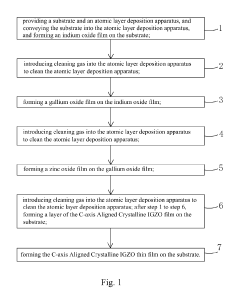
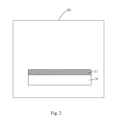
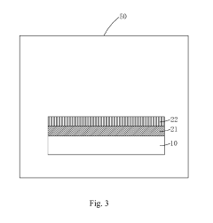
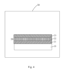
C-axis aligned crystalline IGZO thin film and manufacture method thereof
PatentInactiveUS20190153595A1
Innovation
- A method using atomic layer deposition to form C-axis Aligned Crystalline IGZO thin films by sequentially depositing indium oxide, gallium oxide, and zinc oxide layers on a substrate with controlled temperature, oxygen concentration, and deposition power, resulting in a larger crystalline area with reduced oxygen defects.
Gallium precursors for deposition of gallium-containing oxide films
PatentWO2022266449A1
Innovation
- Development of liquid, non-pyrophoric, halide-free gallium precursors with high vapor pressure, such as (NMe2)2Ga(EtNCH2CH2NMe2), that are thermally stable and compatible with indium and zinc precursors, enabling efficient deposition through vapor deposition processes like ALD and CVD.
Manufacturing Process Differences: Small vs Large IGZO Displays
The manufacturing processes for IGZO (Indium Gallium Zinc Oxide) thin films differ significantly between small and large display applications, primarily due to scaling challenges and end-use requirements. For small displays, such as those in smartphones and tablets, manufacturers typically employ highly precise deposition techniques with stringent uniformity controls. These processes often utilize RF magnetron sputtering with smaller target sizes, allowing for more precise control over film thickness variations, typically maintained within ±2% across the substrate.
In contrast, large display manufacturing requires specialized equipment capable of handling glass substrates exceeding 2.5m × 2.8m for Gen 10.5 fabrication lines. These processes face unique challenges in maintaining uniform deposition across vast areas, often employing multi-chamber inline sputtering systems with larger, sometimes segmented targets. Thickness uniformity tolerances for large displays may extend to ±5%, reflecting the increased difficulty in maintaining consistency across larger areas.
Temperature management represents another critical difference. Small display manufacturing typically operates at higher process temperatures (250-350°C) to achieve optimal crystallinity and performance, whereas large display production often employs lower temperatures (180-250°C) to minimize thermal stress on larger glass substrates, which are more susceptible to warping and dimensional instability.
Annealing procedures also diverge significantly. Small displays benefit from rapid thermal annealing (RTA) processes that can be completed in minutes, while large displays require extended annealing periods, sometimes exceeding several hours, using specialized large-format furnaces with carefully controlled temperature gradients to prevent non-uniform performance characteristics across the panel.
Etching processes present additional distinctions. Small display manufacturing commonly employs wet etching techniques with higher precision requirements, while large display production more frequently utilizes dry etching methods that offer better uniformity across large areas despite potentially lower resolution capabilities. The etch selectivity requirements also differ, with small displays demanding higher selectivity ratios (>100:1) compared to large displays (typically 50:1).
Yield management strategies reflect these fundamental differences. Small display manufacturing emphasizes defect density reduction through class 10 or better cleanroom environments, while large display production focuses on redundancy and repair technologies to address the statistical inevitability of defects across larger areas, operating in less stringent class 100-1000 environments to balance cost considerations with acceptable yield rates.
Energy Efficiency and Performance Metrics Comparison
Energy efficiency represents a critical performance metric when comparing IGZO thin film technology in small versus large display applications. In small displays such as smartphones and tablets, IGZO demonstrates significant power consumption advantages over traditional amorphous silicon (a-Si) technology, typically achieving 80-90% lower power requirements. This efficiency stems from IGZO's higher electron mobility (10-20 times greater than a-Si), which enables faster switching speeds and lower operating voltages.
For large displays like televisions and digital signage, the energy efficiency benefits of IGZO become even more pronounced in absolute terms. Power consumption measurements indicate that IGZO-based large displays can reduce energy usage by 30-40% compared to conventional technologies. This translates to substantial operational cost savings over the product lifecycle, particularly for commercial applications where displays operate continuously.
Response time metrics also show marked differences between small and large IGZO implementations. In small displays, IGZO panels typically achieve response times of 5-10 milliseconds, while large IGZO displays generally range from 8-15 milliseconds. This variance is primarily attributed to the increased capacitance and resistance in larger panel architectures, which slightly impedes electron transport across greater distances.
Brightness efficiency, measured in nits per watt, demonstrates that IGZO maintains relatively consistent performance across different display sizes. However, the technology exhibits superior brightness uniformity in smaller displays, with deviation typically under 5%, compared to 7-12% in larger implementations. This difference becomes particularly noticeable in applications requiring precise color reproduction.
Thermal performance metrics reveal another size-dependent characteristic. Small IGZO displays generate approximately 40% less heat than equivalent a-Si panels, while large IGZO displays show a 25-35% reduction. This differential is attributed to the increased backlight power requirements in larger displays, which contributes proportionally more to overall thermal output.
Refresh rate capabilities also vary significantly between small and large IGZO implementations. Small displays can readily achieve 120Hz or higher refresh rates with minimal power penalties, whereas large IGZO displays typically operate optimally at 60-90Hz before encountering diminishing efficiency returns. This distinction becomes particularly relevant for gaming applications and high-motion content delivery across different device categories.
Unlock deeper insights with Patsnap Eureka Quick Research — get a full tech report to explore trends and direct your research. Try now!
Generate Your Research Report Instantly with AI Agent
Supercharge your innovation with Patsnap Eureka AI Agent Platform!