How IGZO Thin Film Supports Next-Generation Computing Performance
SEP 28, 20259 MIN READ
Generate Your Research Report Instantly with AI Agent
PatSnap Eureka helps you evaluate technical feasibility & market potential.
IGZO Technology Evolution and Performance Objectives
Indium Gallium Zinc Oxide (IGZO) technology represents a significant advancement in semiconductor materials, evolving from traditional amorphous silicon (a-Si) and polycrystalline silicon (poly-Si) technologies. First commercialized in the early 2010s, IGZO has rapidly progressed from a novel material to a critical component in advanced display and computing applications. The evolution of IGZO thin-film transistors (TFTs) has been characterized by continuous improvements in electron mobility, stability, and manufacturing scalability.
The fundamental advantage of IGZO lies in its unique electronic structure, which enables electron mobility 20-50 times higher than conventional a-Si while maintaining low off-state current. This characteristic has positioned IGZO as a transformative technology for both display applications and, increasingly, for next-generation computing architectures. The material's wide bandgap (approximately 3.5 eV) contributes to its exceptional transparency and low leakage current, making it particularly suitable for transparent electronics and low-power applications.
From 2012 to 2017, IGZO development focused primarily on display technologies, with significant advancements in resolution, power efficiency, and form factor flexibility. The period from 2018 to present has witnessed an expansion of IGZO applications into computing domains, particularly in memory arrays, neuromorphic computing elements, and flexible electronics. This transition marks a critical inflection point in IGZO's technological trajectory.
Current technical objectives for IGZO thin films center on several key performance parameters. Researchers aim to achieve electron mobility exceeding 50 cm²/Vs while maintaining stability under bias stress conditions. Reducing the subthreshold swing below 100 mV/decade represents another critical goal to enable lower operating voltages and power consumption. Additionally, enhancing uniformity across large substrates remains essential for industrial-scale production of high-performance computing components.
The roadmap for IGZO technology includes integration with emerging memory technologies such as RRAM (Resistive Random Access Memory) and MRAM (Magnetoresistive Random Access Memory), where IGZO TFTs serve as selector devices. In neuromorphic computing applications, IGZO-based artificial synapses aim to achieve analog weight modulation with precision exceeding 8 bits while consuming less than 1 pJ per operation.
Looking forward, the convergence of IGZO technology with advanced manufacturing techniques, including atomic layer deposition and high-precision patterning, is expected to enable three-dimensional integration of computing elements. This evolution supports the development of vertically stacked memory-logic architectures that promise to overcome the limitations of conventional von Neumann computing paradigms, particularly for data-intensive applications like artificial intelligence and edge computing.
Market Demand Analysis for Advanced Computing Materials
The global computing industry is experiencing unprecedented demand for advanced materials that can support next-generation computing performance. As traditional silicon-based semiconductors approach their physical limitations, the market for alternative materials like IGZO (Indium Gallium Zinc Oxide) thin films is expanding rapidly. Current market analysis indicates that the advanced computing materials sector is projected to reach $25 billion by 2027, with thin-film technologies representing approximately 18% of this market.
The demand for IGZO thin films is primarily driven by the explosive growth in mobile computing devices, high-resolution displays, and emerging technologies such as flexible electronics and Internet of Things (IoT) devices. The global smartphone market, which shipped over 1.3 billion units in 2022, continues to demand thinner, more power-efficient displays where IGZO technology offers significant advantages over conventional amorphous silicon.
Enterprise computing and data center applications represent another substantial market segment. With data centers consuming approximately 1% of global electricity, the energy efficiency benefits of IGZO-based computing components are becoming increasingly attractive. Market research indicates that data center operators can reduce power consumption by up to 30% by implementing IGZO-based technologies in certain applications, creating a compelling value proposition.
The automotive industry is emerging as a significant new market for advanced computing materials. Modern vehicles contain up to 100 million lines of code and dozens of computing systems, with premium vehicles featuring multiple high-resolution displays. This sector's demand for reliable, high-performance, and energy-efficient display and computing technologies is growing at 22% annually, outpacing most other market segments.
Regional analysis reveals that East Asia dominates the manufacturing landscape for advanced computing materials, with Japan, South Korea, and Taiwan collectively accounting for 67% of global production capacity. However, recent geopolitical tensions and supply chain vulnerabilities have accelerated investments in alternative manufacturing locations, with the United States and European Union committing over $50 billion and €43 billion respectively to semiconductor and advanced materials production.
Consumer preferences are also reshaping market demand, with 78% of smartphone users citing battery life as a critical purchase factor. This directly benefits IGZO technology, which can reduce display power consumption by 80-90% compared to conventional technologies. Similarly, the growing market for wearable devices, projected to exceed 500 million units annually by 2025, requires the unique combination of performance, power efficiency, and flexibility that IGZO thin films can provide.
Current IGZO Thin Film Technology Landscape and Barriers
The IGZO (Indium Gallium Zinc Oxide) thin film transistor technology has emerged as a significant advancement in semiconductor materials, currently positioned at a critical juncture in its development trajectory. The global landscape shows varied adoption rates, with Japan and South Korea leading in commercial applications, followed by Taiwan and China rapidly expanding their manufacturing capabilities. Major display manufacturers including Sharp, LG Display, and Samsung have integrated IGZO technology into their production lines, primarily for high-resolution displays and low-power applications.
Despite its promising attributes, IGZO thin film technology faces several substantial barriers to widespread adoption in next-generation computing applications. The most significant challenge remains production scalability, as current manufacturing processes struggle with yield consistency when transitioning to larger substrate sizes or higher throughput requirements. Uniformity across large-area substrates presents particular difficulties, with edge effects and thickness variations compromising performance in commercial-scale production.
Material stability represents another critical barrier, especially for computing applications that demand sustained performance under varying environmental conditions. IGZO films exhibit sensitivity to ambient conditions, with humidity and temperature fluctuations potentially causing threshold voltage shifts and mobility degradation over time. This instability poses serious reliability concerns for long-term computing applications where consistent performance is paramount.
Interface engineering between IGZO and adjacent materials in transistor structures remains problematic, with contact resistance and charge trapping at interfaces limiting overall device performance. These interface phenomena become increasingly significant as device dimensions shrink to meet the demands of advanced computing architectures.
From a manufacturing perspective, the industry faces challenges in standardization of processes and materials. The composition ratios of indium, gallium, and zinc significantly impact electrical properties, yet optimal formulations vary depending on specific applications and processing conditions. This variability complicates the establishment of industry-wide standards necessary for mass production.
Cost factors present additional barriers, particularly the reliance on indium—a relatively scarce element with fluctuating market prices. While IGZO offers advantages over conventional silicon-based technologies in certain applications, the total cost of ownership, including specialized deposition equipment and process optimization, remains higher than established alternatives for many computing applications.
Addressing these technological barriers requires coordinated research efforts across materials science, device engineering, and manufacturing technology domains. Recent developments in atomic layer deposition techniques and post-deposition treatments show promise for improving film quality and stability, potentially overcoming some of the current limitations facing IGZO implementation in next-generation computing systems.
Contemporary IGZO Implementation Architectures
01 IGZO thin film transistor structure optimization
Optimization of IGZO thin film transistor structures can significantly enhance computing performance. This includes modifications to the gate, source, and drain configurations, as well as channel layer engineering. By optimizing these structural elements, key transistor parameters such as carrier mobility, on/off ratio, and threshold voltage stability can be improved, leading to better overall computing performance in devices using IGZO technology.- IGZO thin film transistor structure optimization: Optimizing the structure of IGZO (Indium Gallium Zinc Oxide) thin film transistors can significantly enhance computing performance. This includes modifications to the gate, source, drain configurations, and channel dimensions. Structural improvements such as multi-layer architectures and novel electrode arrangements can reduce parasitic capacitance and resistance, leading to faster switching speeds and improved electron mobility, which are critical for high-performance computing applications.
- Composition and doping techniques for IGZO films: The composition and doping of IGZO films directly impact their electrical properties and computing performance. By adjusting the ratio of indium, gallium, and zinc, or introducing dopants such as hydrogen, nitrogen, or rare earth elements, the carrier concentration and mobility can be optimized. These modifications can enhance the stability of the semiconductor layer, reduce threshold voltage shifts, and improve overall transistor performance for computing applications.
- Deposition and annealing processes for performance enhancement: The methods used for depositing and annealing IGZO thin films significantly affect their crystallinity, defect density, and interface quality. Advanced deposition techniques such as atomic layer deposition, pulsed laser deposition, and RF sputtering with optimized parameters can produce high-quality films. Post-deposition treatments including thermal annealing in various atmospheres (oxygen, nitrogen, forming gas) help reduce oxygen vacancies and improve film uniformity, resulting in enhanced electron mobility and computing performance.
- Integration of IGZO in advanced computing architectures: IGZO thin films can be integrated into various advanced computing architectures including neuromorphic computing systems, memory devices, and flexible electronics. The low off-current and high on/off ratio of IGZO transistors make them suitable for low-power computing applications. When incorporated into 3D stacked structures or combined with other semiconductor materials in heterojunction devices, IGZO-based circuits can achieve higher integration density and improved computational efficiency.
- Stability and reliability enhancements for IGZO-based computing: Improving the stability and reliability of IGZO thin films is crucial for consistent computing performance over time. Techniques such as passivation layers, interface engineering, and bias stress compensation can mitigate threshold voltage shifts and reduce degradation under prolonged operation. Environmental factors like temperature, humidity, and light exposure can be managed through protective encapsulation and circuit design optimizations, ensuring reliable operation of IGZO-based computing devices under various conditions.
02 Material composition and doping techniques
The composition of IGZO materials and various doping techniques play a crucial role in determining computing performance. By adjusting the ratio of indium, gallium, and zinc, or introducing dopants such as hydrogen, nitrogen, or rare earth elements, the electrical properties of IGZO thin films can be tailored. These modifications can enhance carrier concentration, reduce defects, and improve electron mobility, resulting in superior computing performance for electronic devices.Expand Specific Solutions03 Deposition and annealing processes
The methods used for depositing IGZO thin films and subsequent annealing treatments significantly impact computing performance. Various deposition techniques such as sputtering, atomic layer deposition, and solution processing can be employed with different parameters. Post-deposition annealing in controlled atmospheres helps optimize crystal structure, reduce defects, and improve interface quality, all of which contribute to enhanced electrical characteristics and computing performance.Expand Specific Solutions04 Interface engineering and passivation
Engineering the interfaces between IGZO and adjacent layers, along with proper passivation techniques, is essential for maximizing computing performance. By controlling the quality of interfaces with gate dielectrics and implementing effective passivation layers, issues such as charge trapping, interface states, and environmental degradation can be minimized. These approaches lead to improved stability, reliability, and overall computing performance of IGZO-based devices.Expand Specific Solutions05 Circuit design and system integration
Advanced circuit design techniques and system integration approaches can leverage the unique properties of IGZO thin films to enhance computing performance. This includes optimized pixel circuits for displays, novel memory cell architectures, and specialized logic circuits that account for IGZO characteristics. By designing circuits that complement IGZO properties while mitigating limitations, overall system computing performance can be significantly improved in applications ranging from displays to processors.Expand Specific Solutions
Leading IGZO Manufacturers and Research Institutions
IGZO thin film technology is currently in the growth phase of its industry lifecycle, with an expanding market driven by next-generation computing demands. The global market for IGZO displays is projected to reach significant scale as manufacturers seek higher performance, energy-efficient display solutions. Technologically, IGZO has matured beyond early development but continues to evolve, with leading companies at different maturity stages. Sharp and Semiconductor Energy Laboratory pioneered commercial IGZO applications, while BOE, Samsung Display, and AUO have achieved mass production capabilities. TCL China Star Optoelectronics and JUSUNG ENGINEERING are advancing manufacturing processes, while research institutions like Tsinghua University and Imec focus on next-generation implementations. The technology's adoption is accelerating as companies overcome initial yield and stability challenges.
BOE Technology Group Co., Ltd.
Technical Solution: BOE Technology has developed comprehensive IGZO thin-film solutions that significantly enhance next-generation computing performance across multiple applications. Their IGZO implementation features transistors with electron mobility exceeding 15 cm²/Vs, approximately 30 times higher than conventional amorphous silicon, enabling faster response times critical for high-performance computing displays. BOE's manufacturing process incorporates specialized sputtering techniques and precise oxygen partial pressure control during deposition, resulting in optimized film composition and reduced defect density. Their IGZO panels demonstrate remarkable power efficiency, consuming approximately 80-90% less power in static image display scenarios compared to conventional TFT-LCD technology. BOE has successfully integrated IGZO technology into flexible display applications by developing specialized encapsulation techniques that protect the oxide semiconductor from environmental degradation while maintaining flexibility. Their advanced IGZO backplanes support high refresh rates (up to 240Hz) with minimal motion blur, making them ideal for computational applications requiring rapid visual feedback.
Strengths: Comprehensive manufacturing ecosystem allows for vertical integration and quality control; successfully implemented in both rigid and flexible display applications; excellent power efficiency extends battery life in mobile computing devices. Weaknesses: Requires significant capital investment in specialized production equipment; more complex manufacturing process than traditional a-Si; higher sensitivity to environmental factors during production.
Sharp Corp.
Technical Solution: Sharp has pioneered IGZO (Indium Gallium Zinc Oxide) technology as a revolutionary thin-film semiconductor material that significantly enhances computing performance. Their IGZO displays feature electron mobility 20-50 times higher than conventional amorphous silicon, enabling faster response times and higher resolution displays. Sharp's implementation includes ultra-fine pixel designs with transistors approximately 1/10th the size of conventional TFTs, allowing for displays with up to 8K resolution while maintaining exceptional clarity. Their IGZO panels demonstrate remarkable power efficiency, consuming only 1/5 to 1/10 the power of conventional LCD displays when displaying still images, as the oxide semiconductor's unique properties allow transistors to maintain their on/off state with minimal power. Sharp has integrated this technology across various computing platforms, from mobile devices to large format displays, and has developed specialized manufacturing processes that enable mass production while maintaining high yield rates.
Strengths: Industry-leading electron mobility rates provide superior refresh rates and response times; exceptional power efficiency extends battery life in mobile computing applications; enables ultra-high resolution displays with minimal power consumption. Weaknesses: Higher initial manufacturing costs compared to a-Si technology; requires specialized production facilities; more sensitive to certain manufacturing environment conditions.
Critical IGZO Thin Film Patents and Scientific Breakthroughs
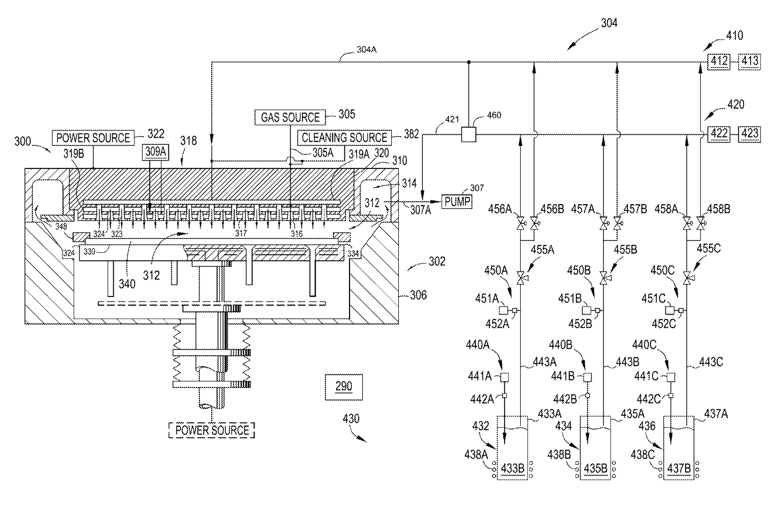
Apparatus and method of forming an indium gallium zinc oxide layer
PatentActiveUS9214340B2
Innovation
- A method and apparatus for forming a multi-element containing film using a gas distribution plate assembly with a precursor plenum and heat exchanging channel, allowing for precise control of precursor gas flow and composition, enabling the deposition of IGZO layers with tailored stoichiometry and reduced environmental exposure.
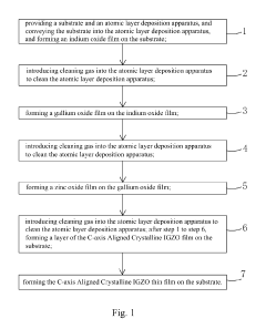
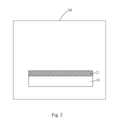
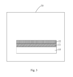
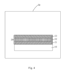
C-axis aligned crystalline IGZO thin film and manufacture method thereof
PatentInactiveUS20190153595A1
Innovation
- A method using atomic layer deposition to form C-axis Aligned Crystalline IGZO thin films by sequentially depositing indium oxide, gallium oxide, and zinc oxide layers on a substrate with controlled temperature, oxygen concentration, and deposition power, resulting in a larger crystalline area with reduced oxygen defects.
Environmental Impact and Sustainability of IGZO Manufacturing
The manufacturing processes of IGZO (Indium Gallium Zinc Oxide) thin films present both environmental challenges and sustainability opportunities that warrant careful consideration as this technology becomes increasingly central to next-generation computing devices. The production of IGZO involves several rare earth elements, particularly indium, which faces significant supply constraints and geopolitical extraction challenges. Current mining practices for these materials often result in substantial environmental degradation, including soil contamination, water pollution, and habitat destruction in extraction regions.
Energy consumption represents another critical environmental concern in IGZO manufacturing. The deposition processes—primarily sputtering and chemical vapor deposition—require considerable energy inputs, contributing to the carbon footprint of electronic devices. However, compared to traditional silicon-based semiconductor manufacturing, IGZO production typically operates at lower temperatures, potentially reducing overall energy requirements by 30-40% according to recent industry analyses.
Water usage in IGZO fabrication facilities presents both challenges and improvements over conventional semiconductor manufacturing. While the cleaning and processing steps still demand significant water resources, the simplified structure of IGZO transistors requires fewer processing steps, potentially reducing water consumption by up to 25% compared to traditional silicon-based technologies.
Waste management in IGZO production presents particular sustainability challenges due to the presence of heavy metals and chemical compounds used in the manufacturing process. Industry leaders have begun implementing closed-loop recycling systems that can recover up to 60% of indium from production waste, significantly reducing the demand for virgin materials while minimizing hazardous waste generation.
The longevity benefits of IGZO-based devices offer substantial sustainability advantages. The superior electron mobility and lower power consumption of IGZO transistors extend device operational lifespans by approximately 30-40%, reducing electronic waste generation. Additionally, the technology's compatibility with flexible substrates enables thinner, more durable device designs that can withstand physical stress better than conventional rigid electronics.
Several manufacturers have begun implementing green chemistry principles in IGZO production, developing water-based precursors and less toxic chemical alternatives that reduce environmental impact while maintaining performance specifications. These innovations, coupled with industry-wide efforts to establish responsible supply chains for rare earth elements, demonstrate promising progress toward more sustainable IGZO manufacturing practices that can support the growing demand for high-performance, energy-efficient computing devices.
Integration Challenges with Existing Semiconductor Technologies
The integration of IGZO (Indium Gallium Zinc Oxide) thin film technology with existing semiconductor manufacturing processes presents significant challenges that must be addressed to fully realize its potential in next-generation computing applications. Traditional silicon-based semiconductor fabrication has been optimized over decades, creating established processes that new materials must adapt to or overcome.
Temperature sensitivity represents one of the primary integration hurdles. While silicon can withstand high-temperature processing (often exceeding 1000°C), IGZO thin films typically degrade at temperatures above 300-350°C. This thermal constraint limits compatibility with standard CMOS fabrication steps, particularly high-temperature annealing processes, necessitating the development of low-temperature alternatives or specialized integration sequences.
Interface engineering between IGZO and conventional semiconductor materials presents another critical challenge. Contact resistance issues at the interface between IGZO and metal electrodes can significantly degrade device performance. The formation of stable, low-resistance contacts requires careful material selection and process optimization to ensure efficient charge transfer across these boundaries.
Contamination control during integration poses substantial difficulties. IGZO is particularly sensitive to hydrogen and water vapor contamination, which can alter its electrical properties by creating oxygen vacancies or hydroxyl groups. Existing semiconductor fabrication environments must be modified to accommodate these sensitivities, often requiring specialized encapsulation layers or modified process chambers.
Scaling considerations further complicate integration efforts. While IGZO offers excellent performance at larger feature sizes, maintaining consistent electrical characteristics becomes increasingly challenging as dimensions shrink below 10nm. This scaling limitation conflicts with the semiconductor industry's continuous drive toward miniaturization, requiring novel device architectures or hybrid approaches.
Uniformity and reproducibility across large substrates represent additional integration challenges. Achieving consistent IGZO film properties over 300mm wafers or larger glass substrates demands precise control of deposition parameters. Variations in film thickness, composition, or microstructure can lead to device-to-device performance variations that are unacceptable in high-performance computing applications.
Equipment compatibility issues also emerge when introducing IGZO into established semiconductor fabrication lines. Many existing tools are optimized for silicon processing and may require significant modifications or replacements to accommodate IGZO's unique material properties and processing requirements, adding substantial capital costs to integration efforts.
Unlock deeper insights with PatSnap Eureka Quick Research — get a full tech report to explore trends and direct your research. Try now!
Generate Your Research Report Instantly with AI Agent
Supercharge your innovation with PatSnap Eureka AI Agent Platform!