IGZO Thin Film: Cross-Industry Application Potential Analysis
SEP 28, 202510 MIN READ
Generate Your Research Report Instantly with AI Agent
Patsnap Eureka helps you evaluate technical feasibility & market potential.
IGZO Technology Background and Development Goals
Indium Gallium Zinc Oxide (IGZO) thin film technology represents a significant advancement in semiconductor materials, emerging as a promising alternative to conventional amorphous silicon (a-Si) and low-temperature polysilicon (LTPS) technologies. First developed in the early 2000s by researchers at Tokyo Institute of Technology, IGZO belongs to the family of transparent amorphous oxide semiconductors (TAOS) that combine transparency with electrical conductivity properties.
The evolution of IGZO technology has been driven by increasing demands for higher performance displays with lower power consumption. Traditional a-Si technology, while cost-effective, suffers from limited electron mobility (typically <1 cm²/Vs), restricting its application in high-resolution displays. IGZO addresses this limitation by offering 10-50 times higher electron mobility (10-20 cm²/Vs), enabling faster switching speeds and higher resolution displays while maintaining transparency.
Sharp Corporation pioneered the commercial application of IGZO in 2012, introducing the first IGZO-based LCD panels. This milestone marked the beginning of IGZO's industrial adoption, which has since expanded beyond displays to various electronic applications. The technology's development trajectory has been characterized by continuous improvements in deposition techniques, material composition optimization, and manufacturing scalability.
The fundamental advantage of IGZO lies in its unique electronic structure. Unlike silicon-based semiconductors, IGZO's conduction band is primarily composed of spherical s-orbitals of metal cations, which overlap effectively even in amorphous states. This structure enables high electron mobility despite the material's amorphous nature, combining the performance benefits of crystalline materials with the manufacturing advantages of amorphous ones.
Current development goals for IGZO technology focus on several key areas. First, researchers aim to further enhance electron mobility while maintaining stability, with targets exceeding 50 cm²/Vs for specialized applications. Second, improving the technology's compatibility with flexible substrates represents a critical objective for enabling next-generation flexible electronics. Third, reducing manufacturing costs through optimized deposition processes and equipment is essential for broader market adoption.
Additionally, the industry is pursuing enhanced stability under various environmental conditions, particularly regarding temperature fluctuations and prolonged light exposure. Researchers are also exploring novel doping strategies and compositional variations to tailor IGZO properties for specific applications beyond displays, including sensors, memory devices, and integrated circuits.
The cross-industry potential of IGZO technology stems from its unique combination of transparency, high electron mobility, low-temperature processing capability, and compatibility with large-area fabrication methods. These attributes position IGZO as a key enabling technology for the next generation of electronics spanning multiple sectors, from consumer electronics to healthcare, automotive, and industrial applications.
Market Demand Analysis for IGZO Thin Film Applications
The IGZO (Indium Gallium Zinc Oxide) thin film market is experiencing robust growth driven by increasing demand for high-performance display technologies. The global market for IGZO-based products was valued at approximately $2.3 billion in 2022 and is projected to grow at a compound annual growth rate of 15.8% through 2028, reaching an estimated $5.6 billion by the end of the forecast period.
The display industry represents the primary demand driver for IGZO technology, with manufacturers seeking solutions that offer higher electron mobility, better transparency, and lower power consumption compared to traditional amorphous silicon (a-Si) technology. Major display manufacturers including Samsung, LG Display, and Sharp have already incorporated IGZO technology into their premium product lines, signaling strong industry adoption.
Consumer electronics, particularly smartphones and tablets, constitute the largest application segment for IGZO thin films. The technology's ability to deliver higher resolution displays while consuming less power aligns perfectly with consumer demands for devices with extended battery life and superior visual quality. Market research indicates that approximately 38% of premium smartphones launched in 2023 incorporated some form of IGZO technology, up from 24% in 2021.
Beyond consumer electronics, significant growth potential exists in emerging application areas. The healthcare sector shows increasing interest in IGZO for medical imaging displays, where high resolution and reliability are critical. The automotive industry represents another high-potential market, with IGZO-based displays being integrated into advanced dashboard systems and entertainment consoles in premium vehicle models.
The semiconductor and sensor industries are exploring IGZO for next-generation thin-film transistors and transparent electronics applications. Market analysts predict that these non-display applications could grow to represent 25% of the total IGZO market by 2027, compared to less than 10% currently.
Regionally, East Asia dominates the IGZO market with approximately 65% market share, driven by the concentration of display manufacturing facilities in countries like South Korea, Japan, and Taiwan. However, North America and Europe are showing accelerated adoption rates, particularly in specialized applications such as medical devices and aerospace instrumentation.
Supply chain considerations are increasingly influencing market dynamics, with concerns about indium availability and price volatility affecting long-term planning. This has spurred research into alternative compositions that maintain performance while reducing dependence on scarce materials, creating additional market opportunities for innovative material solutions.
IGZO Technical Challenges and Global Development Status
IGZO (Indium Gallium Zinc Oxide) thin film technology faces several significant technical challenges despite its promising applications across multiple industries. The primary challenge lies in the stability of IGZO semiconductors, particularly under prolonged bias stress and varying environmental conditions. When exposed to light, humidity, or temperature fluctuations, IGZO displays can experience threshold voltage shifts and carrier mobility degradation, affecting long-term performance reliability.
Manufacturing scalability presents another substantial hurdle. While IGZO offers advantages over amorphous silicon (a-Si) and low-temperature polysilicon (LTPS), achieving uniform deposition across large substrates remains difficult. The precise control of oxygen vacancies—critical for determining electrical properties—requires sophisticated deposition techniques and post-processing treatments that are challenging to implement in mass production environments.
Contact resistance issues at the interface between IGZO and electrode materials continue to limit device performance, particularly in high-frequency applications. This challenge becomes more pronounced as device dimensions shrink, necessitating novel interface engineering solutions.
Globally, IGZO technology development demonstrates distinct regional characteristics. Japan maintains leadership through companies like Sharp and semiconductor equipment manufacturers, having pioneered much of the fundamental research. South Korea has leveraged IGZO for advanced display technologies, with Samsung and LG making significant investments in production capabilities.
Taiwan has established itself as a manufacturing hub for IGZO-based displays, with companies like AU Optronics and Innolux Corporation developing competitive production processes. China has rapidly expanded its IGZO manufacturing capacity, supported by government initiatives to build domestic display technology capabilities.
In the United States and Europe, research efforts focus primarily on next-generation applications beyond displays, including flexible electronics, sensors, and neuromorphic computing. These regions emphasize innovation in materials science and device architecture rather than mass production capabilities.
Academic and industrial collaboration varies significantly by region. Asian countries demonstrate stronger industry-academia partnerships specifically targeted at manufacturing optimization, while Western research institutions tend to focus on fundamental materials science and novel applications. This geographical distribution of expertise has created specialized knowledge centers, with material synthesis innovations concentrated in Japan and the United States, while process optimization expertise is stronger in Taiwan and South Korea.
The technical challenges facing IGZO technology are gradually being addressed through international research efforts, though solutions that balance performance, cost, and manufacturing scalability remain elusive for certain applications, particularly those requiring extreme reliability or flexibility.
Current IGZO Implementation Solutions and Techniques
01 IGZO thin film fabrication methods
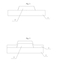
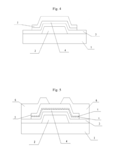
Various methods for fabricating IGZO (Indium Gallium Zinc Oxide) thin films are disclosed, including sputtering, chemical vapor deposition, and solution processing techniques. These methods focus on controlling the deposition parameters to achieve optimal film properties such as thickness uniformity, crystallinity, and electrical characteristics. The fabrication processes often involve specific temperature treatments and atmospheric conditions to enhance the semiconductor performance of the resulting IGZO films.- IGZO thin film composition and structure: IGZO (Indium Gallium Zinc Oxide) thin films are semiconductor materials composed of indium, gallium, zinc, and oxygen. The composition ratio of these elements significantly affects the electrical properties of the film. Various deposition techniques are used to create IGZO thin films with specific structural characteristics, including crystalline or amorphous phases. The microstructure of these films can be engineered to optimize carrier mobility, stability, and other semiconductor properties essential for electronic device applications.
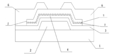
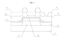
- IGZO thin film transistor (TFT) fabrication methods: Fabrication methods for IGZO thin film transistors involve multiple processing steps including substrate preparation, film deposition, patterning, and annealing treatments. Techniques such as sputtering, chemical vapor deposition, and solution processing are commonly employed to deposit IGZO layers. Post-deposition treatments including thermal annealing, plasma treatment, and passivation layers are critical for optimizing TFT performance. These methods aim to control defects, improve interface quality, and enhance electrical characteristics such as mobility, threshold voltage stability, and on/off current ratio.
- IGZO thin film applications in display technology: IGZO thin films are widely used in display technologies due to their high electron mobility and transparency. They serve as the active semiconductor layer in thin film transistors for OLED and LCD displays, enabling higher resolution, faster refresh rates, and lower power consumption compared to conventional amorphous silicon. IGZO-based backplanes support advanced display features such as high dynamic range, flexible/foldable screens, and transparent displays. The material's stability and performance characteristics make it particularly suitable for next-generation display applications requiring high pixel density and energy efficiency.
- IGZO thin film performance enhancement techniques: Various techniques are employed to enhance IGZO thin film performance, including doping with additional elements, interface engineering, and multilayer structures. Oxygen vacancy control through annealing in specific atmospheres helps optimize carrier concentration. Surface passivation layers protect IGZO films from environmental degradation and reduce threshold voltage instability. Advanced deposition parameters and post-treatment processes can significantly improve electrical characteristics such as field-effect mobility, subthreshold swing, and bias stress stability, leading to better overall device performance and reliability.
- IGZO thin film integration with emerging technologies: IGZO thin films are being integrated with emerging technologies including flexible electronics, sensors, and neuromorphic computing systems. The material's compatibility with low-temperature processing enables its application on flexible substrates such as plastic and metal foils. IGZO-based devices are being developed for transparent electronics, wearable technology, and IoT applications. Research is also focused on combining IGZO with other functional materials to create novel heterostructures for advanced electronic and optoelectronic applications, including memristors, photodetectors, and energy harvesting devices.
02 IGZO thin film transistor structures
Different structural designs for IGZO-based thin film transistors (TFTs) are presented, including bottom-gate, top-gate, and dual-gate configurations. These structures incorporate various electrode materials, dielectric layers, and channel geometries to optimize device performance. The transistor designs aim to improve key parameters such as mobility, on/off ratio, threshold voltage stability, and operational reliability for applications in display technologies and integrated circuits.Expand Specific Solutions03 IGZO composition and doping strategies
Innovations in IGZO material composition and doping approaches are described, focusing on modifying the In:Ga:Zn ratio and incorporating additional elements to enhance specific properties. Doping strategies include the addition of elements such as aluminum, hafnium, or nitrogen to improve stability, carrier concentration, and mobility. These compositional modifications aim to address common challenges in IGZO films such as oxygen vacancy formation, bias stress instability, and environmental sensitivity.Expand Specific Solutions04 IGZO thin film applications in display technology
Applications of IGZO thin films in display technologies are detailed, particularly focusing on their implementation in active-matrix displays such as OLED and LCD panels. The advantages of IGZO for displays include high electron mobility, low off-current, transparency, and compatibility with large-area fabrication. These properties enable the development of high-resolution, energy-efficient displays with improved refresh rates and reduced power consumption for various consumer electronic devices.Expand Specific Solutions05 IGZO thin film reliability and passivation techniques
Methods for improving the reliability and stability of IGZO thin films through passivation and encapsulation techniques are presented. These approaches include the application of protective layers, surface treatments, and interface engineering to mitigate environmental degradation and bias stress effects. Passivation strategies focus on reducing oxygen vacancy formation, preventing moisture ingress, and stabilizing the semiconductor-dielectric interface to extend device lifetime and maintain consistent performance under various operating conditions.Expand Specific Solutions
Key Industry Players in IGZO Thin Film Development
The IGZO thin film technology market is currently in a growth phase, characterized by expanding applications across display, semiconductor, and electronics industries. The market is projected to reach significant scale due to IGZO's superior electron mobility, transparency, and power efficiency compared to traditional materials. Leading display manufacturers including Samsung Display, LG Display, BOE Technology, Sharp, and TCL China Star Optoelectronics are driving commercial adoption, while research institutions like Interuniversitair Micro-Electronica Centrum and universities (Southeast, Nankai) are advancing fundamental innovations. Equipment suppliers such as ULVAC and JUSUNG ENGINEERING provide critical manufacturing infrastructure. The technology has reached commercial maturity in display applications but remains in development for emerging cross-industry applications, with companies like Canon and Intermolecular pursuing novel implementations beyond displays.
ULVAC INC
Technical Solution: ULVAC has developed specialized deposition equipment and processes specifically optimized for IGZO thin film production. Their approach centers on advanced sputtering technology that achieves precise control over film composition, thickness uniformity, and defect density. ULVAC's implementation includes proprietary target materials with optimized indium-gallium-zinc ratios and specialized sputtering cathodes that enhance deposition uniformity across large substrates. Their equipment achieves exceptional thickness variation control (±2% across Gen 10+ substrates) while maintaining high throughput necessary for commercial production. ULVAC has pioneered multi-chamber in-line sputtering systems that enable continuous IGZO deposition with controlled atmosphere transitions, significantly reducing contamination risks. Their technology supports both rigid and flexible substrate processing, with specialized solutions for temperature-sensitive materials. Recent innovations include developing cluster-type sputtering systems with integrated annealing capabilities that optimize IGZO electrical properties in-situ, reducing the need for separate post-deposition treatments.
Strengths: Industry-leading expertise in deposition equipment; comprehensive process knowledge; ability to support various substrate types and sizes. Weaknesses: Limited to equipment/process side of the value chain; dependent on display manufacturers' technology adoption rates; high equipment costs requiring significant capital investment from customers.
BOE Technology Group Co., Ltd.
Technical Solution: BOE has developed comprehensive IGZO technology solutions targeting both display and non-display applications. Their approach focuses on flexible IGZO backplanes with high electron mobility (12-18 cm²/Vs) achieved through optimized sputtering processes and post-deposition annealing techniques. BOE's implementation incorporates proprietary metal oxide compositions that enhance stability while maintaining high transparency (>90% in visible spectrum). Their manufacturing process achieves exceptional uniformity across Gen 10.5 substrates, enabling cost-effective production of large-area displays with minimal variation. BOE has successfully commercialized IGZO technology in premium LCD and OLED displays, achieving significant power reductions while maintaining high refresh rates. Beyond displays, BOE has pioneered IGZO applications in X-ray imaging sensors, achieving significantly higher sensitivity than conventional a-Si sensors. Recent innovations include developing hybrid IGZO-LTPS backplanes that combine the advantages of both technologies and implementing IGZO in touch-integrated display panels to reduce overall module thickness.
Strengths: Extensive manufacturing capacity; vertical integration capabilities; strong position in both display and sensor applications. Weaknesses: Challenges with yield optimization at largest substrate sizes; sensitivity to process variations; higher material costs compared to conventional a-Si.
Core IGZO Thin Film Patents and Technical Innovations
C-axis aligned crystalline IGZO thin film and manufacture method thereof
PatentInactiveUS20190153595A1
Innovation
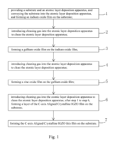
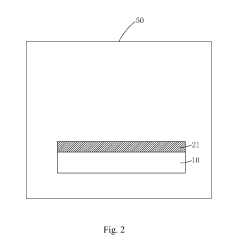
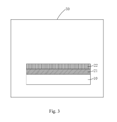
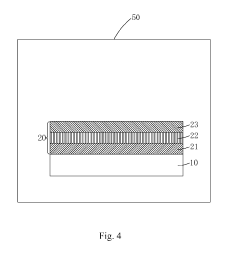
- A method using atomic layer deposition to form C-axis Aligned Crystalline IGZO thin films by sequentially depositing indium oxide, gallium oxide, and zinc oxide layers on a substrate with controlled temperature, oxygen concentration, and deposition power, resulting in a larger crystalline area with reduced oxygen defects.
Thin film transistor and method of fabricating the same, display substrate and display device
PatentInactiveUS20150311345A1
Innovation
- A method involving the formation of an oxide active layer and a tin oxide-based protective layer on a substrate, where both layers are patterned in a single process, and annealed in an oxygen-containing atmosphere to create transitional regions that reduce off-state current, eliminating the need for via holes and simplifying the manufacturing procedure.
Supply Chain Analysis for IGZO Manufacturing
The IGZO (Indium Gallium Zinc Oxide) manufacturing supply chain represents a complex ecosystem involving multiple stakeholders across various geographical regions. Raw material sourcing forms the foundation of this chain, with indium being particularly critical due to its limited global reserves. China currently dominates indium production, accounting for approximately 60% of global supply, followed by South Korea and Japan. This geographical concentration creates potential supply vulnerabilities that manufacturers must strategically address through diversification efforts and long-term procurement contracts.
Processing these raw materials into high-purity compounds suitable for thin-film deposition requires specialized equipment and expertise. Key equipment manufacturers include Applied Materials, Tokyo Electron, and ULVAC, who provide the advanced physical vapor deposition (PVD) and chemical vapor deposition (CVD) systems essential for IGZO fabrication. These equipment providers have established strong positions in the market, with Japanese and American companies holding significant intellectual property portfolios related to deposition technologies.
The manufacturing process itself involves multiple stages, from substrate preparation to thin-film deposition, patterning, and encapsulation. This complexity necessitates tight integration between material suppliers, equipment manufacturers, and end-product fabricators. Display manufacturers like Samsung, LG Display, and Sharp have developed vertically integrated operations to maintain quality control throughout the production process, while smaller players often rely on partnerships with specialized suppliers.
Quality control represents a significant challenge in the IGZO supply chain, as even minor impurities can dramatically affect semiconductor performance. Advanced metrology and testing equipment from providers such as KLA-Tencor and Hitachi High-Technologies play crucial roles in maintaining production standards. The increasing demand for higher-resolution displays and more sophisticated semiconductor applications has driven continuous improvement in quality control methodologies.
Supply chain resilience has become a strategic priority following recent global disruptions. Companies are increasingly implementing dual-sourcing strategies for critical materials and components, while also exploring alternative material systems that could reduce dependence on scarce elements like indium. Additionally, regional manufacturing clusters have emerged in East Asia, particularly in South Korea, Taiwan, and Japan, creating ecosystems that facilitate knowledge sharing and supply chain efficiency.
Cost structures within the IGZO manufacturing chain remain heavily influenced by raw material prices, equipment depreciation, and yield rates. As production scales increase, particularly for display applications, economies of scale are gradually reducing manufacturing costs, though high-purity material requirements continue to present cost challenges for specialized applications beyond the display industry.
Environmental Impact and Sustainability of IGZO Technology
The environmental impact of IGZO (Indium Gallium Zinc Oxide) technology presents a complex sustainability profile that merits careful consideration as its cross-industry applications expand. IGZO thin films offer significant environmental advantages compared to conventional semiconductor materials, primarily through reduced power consumption. Devices incorporating IGZO technology typically require 80-90% less power than their amorphous silicon counterparts, translating to extended battery life in portable electronics and reduced energy demands in large-scale display installations.
This energy efficiency contributes substantially to sustainability goals by decreasing carbon footprints across multiple industries. For instance, IGZO-based displays in consumer electronics can reduce global energy consumption by an estimated 0.5-1% if widely adopted, representing a significant contribution to climate change mitigation efforts.
Material considerations present both challenges and opportunities for IGZO sustainability. The technology utilizes indium, a relatively scarce element with limited global reserves estimated at 15,000 metric tons. Current extraction practices for indium are often environmentally problematic, involving energy-intensive processes and generating hazardous waste. However, IGZO films require significantly less material than traditional semiconductor layers, with typical thicknesses of only 30-50 nanometers, minimizing resource demands.
Manufacturing processes for IGZO thin films have evolved toward greater sustainability. Modern deposition techniques such as room-temperature sputtering consume substantially less energy than high-temperature processes required for silicon-based semiconductors. Additionally, IGZO production generally involves fewer toxic chemicals and generates less hazardous waste than conventional semiconductor manufacturing.
End-of-life considerations reveal further environmental advantages. IGZO components contain valuable recoverable materials, particularly indium, which can be reclaimed through emerging recycling technologies. Several research initiatives are developing efficient methods for recovering indium from electronic waste, potentially creating closed-loop material cycles that would significantly enhance the technology's sustainability profile.
Regulatory frameworks worldwide are increasingly recognizing IGZO's environmental benefits. The European Union's Eco-design Directive and similar policies in Asia and North America have begun incorporating energy efficiency standards that indirectly favor IGZO-based technologies. These regulatory trends are likely to accelerate IGZO adoption while simultaneously driving further sustainability improvements in its production and application.
Future sustainability improvements for IGZO technology will likely focus on developing alternative material compositions that reduce dependence on scarce elements while maintaining performance characteristics. Research into gallium-free or indium-reduced formulations shows promising results, potentially addressing resource constraints while preserving the technology's environmental benefits.
Unlock deeper insights with Patsnap Eureka Quick Research — get a full tech report to explore trends and direct your research. Try now!
Generate Your Research Report Instantly with AI Agent
Supercharge your innovation with Patsnap Eureka AI Agent Platform!