Research on IGZO Thin Film Deposition Techniques
SEP 28, 20259 MIN READ
Generate Your Research Report Instantly with AI Agent
Patsnap Eureka helps you evaluate technical feasibility & market potential.
IGZO Thin Film Technology Background and Objectives
Indium Gallium Zinc Oxide (IGZO) thin film technology represents a significant advancement in semiconductor materials, emerging in the early 2000s as a promising alternative to conventional amorphous silicon (a-Si) and polycrystalline silicon (poly-Si) technologies. The evolution of IGZO began with the pioneering work of Hosono and colleagues at the Tokyo Institute of Technology in 2004, who demonstrated that this transparent amorphous oxide semiconductor could achieve electron mobility significantly higher than a-Si while maintaining excellent uniformity and low processing temperatures.
The technological trajectory of IGZO has been characterized by continuous improvements in deposition techniques, material composition optimization, and device integration strategies. Initially developed primarily for thin-film transistors (TFTs) in display applications, IGZO technology has expanded its potential use cases to include sensors, memory devices, and flexible electronics. This expansion has been driven by IGZO's unique combination of high electron mobility, optical transparency, and compatibility with low-temperature processing.
Current research trends in IGZO thin film deposition focus on several key areas: enhancing material stability under environmental stresses, reducing defect densities, improving interface quality with dielectric materials, and developing scalable deposition methods suitable for large-area manufacturing. The field has witnessed a shift from laboratory-scale demonstrations to industrial implementation, particularly in high-resolution display production.
The primary technical objectives for IGZO thin film deposition research include developing precise control over film stoichiometry, achieving uniform deposition over large areas, minimizing defect formation, and ensuring compatibility with flexible substrates. Researchers aim to establish reproducible processes that can deliver consistent electrical performance while maintaining low production costs. Additionally, there is growing interest in environmentally friendly deposition approaches that reduce the use of toxic precursors and minimize energy consumption.
Looking forward, the technology roadmap for IGZO thin films points toward integration with emerging technologies such as quantum computing components, neuromorphic computing elements, and advanced bioelectronic interfaces. The convergence of IGZO with other advanced materials, such as 2D semiconductors and organic electronics, represents a frontier with significant potential for disruptive innovation. As display technology continues to evolve toward higher resolutions, lower power consumption, and novel form factors, IGZO thin film technology is positioned to play an increasingly central role in enabling these advancements.
Market Demand Analysis for IGZO Applications
The IGZO (Indium Gallium Zinc Oxide) thin film market has experienced significant growth driven by the expanding display industry. The global demand for IGZO-based displays has been steadily increasing due to their superior performance characteristics compared to conventional amorphous silicon (a-Si) technology. IGZO offers higher electron mobility, lower power consumption, and better transparency, making it particularly attractive for high-resolution displays and energy-efficient applications.
The display industry represents the primary market for IGZO technology, with applications spanning smartphones, tablets, televisions, and computer monitors. As consumers increasingly demand higher resolution displays with reduced power consumption, manufacturers are turning to IGZO as a solution. The smartphone segment particularly shows strong growth potential, as IGZO enables thinner devices with longer battery life and improved touch response.
Beyond consumer electronics, emerging applications in healthcare, automotive displays, and industrial monitoring systems are creating new market opportunities for IGZO technology. Medical imaging displays benefit from IGZO's high resolution and low power consumption, while automotive heads-up displays leverage its transparency and reliability under varying temperature conditions.
Market analysis indicates that the Asia-Pacific region dominates IGZO production and implementation, with Japan, South Korea, and Taiwan leading in manufacturing capacity. However, significant investments in China are rapidly expanding production capabilities in the region. North America and Europe represent important markets for end products incorporating IGZO technology, particularly in premium consumer electronics and specialized industrial applications.
The global IGZO market is projected to grow substantially over the next five years, driven by increasing adoption in flexible displays, transparent electronics, and next-generation wearable devices. The shift toward Internet of Things (IoT) devices and smart home technologies presents additional growth vectors, as these applications benefit from IGZO's low power requirements and performance stability.
Market challenges include the relatively high cost of indium as a raw material and competition from alternative technologies such as LTPS (Low-Temperature Polysilicon) and organic semiconductors. Environmental concerns regarding indium mining and processing also present potential regulatory hurdles that may impact market dynamics.
Industry experts anticipate that continued improvements in IGZO deposition techniques will be crucial for market expansion, as more efficient and cost-effective manufacturing processes would enable broader adoption across price-sensitive market segments. The development of scalable, high-yield deposition methods represents a key factor in determining the technology's future market penetration and commercial success.
Current Status and Challenges in IGZO Deposition
IGZO (Indium Gallium Zinc Oxide) thin film deposition technology has evolved significantly over the past decade, with various techniques being developed and refined. Currently, the most widely adopted methods include sputtering, pulsed laser deposition (PLD), atomic layer deposition (ALD), and solution-based processes. Among these, RF magnetron sputtering dominates commercial applications due to its scalability, uniformity, and compatibility with existing manufacturing infrastructure.
The global landscape of IGZO deposition technology shows regional specialization. Japan leads in commercial implementation, with companies like Sharp and SEL pioneering large-scale production. South Korea follows closely with Samsung and LG Display making significant advancements. China has rapidly expanded its research capabilities, while European and North American institutions focus more on fundamental research and novel deposition techniques.
Despite progress, several critical challenges persist in IGZO thin film deposition. Oxygen vacancy control remains one of the most significant issues, as these vacancies dramatically influence carrier concentration and mobility. Achieving precise stoichiometry across large substrates presents another major hurdle, particularly as display manufacturers move toward Gen 10+ substrates exceeding 3 meters in width.
Temperature sensitivity constitutes another key challenge. While lower processing temperatures (below 300°C) are desirable for flexible substrate compatibility, they often result in films with inferior electrical properties. Conversely, higher temperature processes that yield better performance are incompatible with temperature-sensitive substrates like polymers.
Uniformity across large areas represents a persistent manufacturing challenge. Current deposition techniques struggle to maintain consistent film thickness and composition across increasingly larger substrates, leading to performance variations in finished devices. This becomes particularly problematic for high-resolution displays where pixel-to-pixel consistency is crucial.
Stability issues also plague IGZO technology, with films often exhibiting performance degradation under environmental stresses such as humidity, temperature fluctuations, and prolonged bias stress. This necessitates additional passivation layers and protective measures, increasing production complexity and cost.
The industry also faces sustainability challenges related to indium supply. As a relatively rare element with growing demand across multiple industries, indium availability and price volatility pose long-term concerns for IGZO scalability. Research into reducing indium content or finding alternative materials has intensified as a result.
Equipment scaling presents another significant barrier, particularly for emerging techniques like ALD. While these methods offer superior film quality and thickness control, their throughput limitations make them less attractive for high-volume manufacturing environments where production efficiency is paramount.
Current IGZO Deposition Methodologies
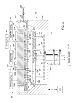
01 Sputtering deposition methods for IGZO thin films
Sputtering is a widely used technique for depositing IGZO (Indium Gallium Zinc Oxide) thin films. This process involves bombarding a target material with high-energy particles, causing atoms to be ejected and deposited onto a substrate. Various sputtering parameters such as power, pressure, and gas composition can be adjusted to control the properties of the resulting IGZO film. This method allows for precise control of film thickness and composition, which are critical factors affecting the performance of IGZO-based electronic devices.- Sputtering deposition techniques for IGZO thin films: Sputtering is a widely used technique for depositing IGZO (Indium Gallium Zinc Oxide) thin films. This process involves bombarding a target material with energetic particles, causing atoms to be ejected and deposited onto a substrate. Various sputtering methods, including RF magnetron sputtering and DC sputtering, can be employed to achieve high-quality IGZO films with controlled composition and thickness. Process parameters such as power, pressure, and gas flow rates significantly influence the film properties.
- Chemical vapor deposition methods for IGZO: Chemical vapor deposition (CVD) techniques offer an alternative approach for IGZO thin film fabrication. In these processes, precursor gases react or decompose on the substrate surface to form the desired film. Variants include atomic layer deposition (ALD), which provides precise thickness control through sequential self-limiting reactions, and metal-organic chemical vapor deposition (MOCVD), which uses organometallic precursors. These methods can produce highly uniform IGZO films with excellent step coverage and can be performed at lower temperatures than some physical deposition techniques.
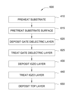
- Post-deposition treatment of IGZO films: Post-deposition treatments are crucial for optimizing the electrical and structural properties of IGZO thin films. Thermal annealing in various atmospheres (oxygen, nitrogen, forming gas) can reduce defects, improve crystallinity, and enhance carrier mobility. Plasma treatments can modify surface properties and reduce oxygen vacancies. Other treatments include laser annealing and high-pressure annealing. These processes significantly impact the performance of IGZO-based devices by controlling oxygen vacancy concentration and improving film stability.
- Composition control and doping strategies for IGZO: Controlling the composition and incorporating dopants in IGZO films are essential for tailoring their electrical properties. The In:Ga:Zn ratio significantly affects carrier concentration, mobility, and stability. Various dopants can be introduced during deposition to modify band structure, enhance conductivity, or improve stability. Co-sputtering from multiple targets or using composite targets with specific compositions allows precise control over the film stoichiometry. These approaches enable customization of IGZO properties for specific applications in display technologies and electronics.
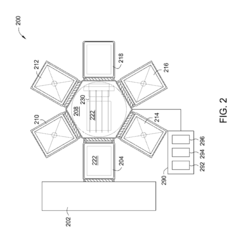
- Novel deposition equipment and process innovations: Advanced equipment designs and process innovations continue to improve IGZO thin film deposition. Multi-chamber systems allow for in-situ deposition of multilayer structures without vacuum breaking. Roll-to-roll processing enables continuous deposition on flexible substrates. Other innovations include high-density plasma sources for enhanced film quality, substrate rotation mechanisms for improved uniformity, and real-time monitoring systems for process control. These technological advancements support the manufacturing of high-performance IGZO-based devices with improved throughput and reduced costs.
02 Chemical vapor deposition techniques for IGZO
Chemical vapor deposition (CVD) techniques offer an alternative approach for IGZO thin film formation. In this process, precursor gases react or decompose on the substrate surface to form the desired IGZO film. Various CVD methods including atomic layer deposition (ALD) can be employed to achieve highly uniform and conformal IGZO films with precise thickness control. These techniques allow for lower deposition temperatures compared to some other methods, which can be beneficial for temperature-sensitive substrates used in flexible electronics applications.Expand Specific Solutions03 Post-deposition treatment of IGZO films
Post-deposition treatments are crucial for optimizing the electrical and structural properties of IGZO thin films. These treatments include thermal annealing in various atmospheres (oxygen, nitrogen, forming gas), plasma treatments, and laser annealing. Such processes help to reduce defects, improve crystallinity, adjust carrier concentration, and enhance mobility in the IGZO layer. The selection of appropriate post-deposition treatment conditions significantly impacts the performance and stability of IGZO-based transistors and other electronic devices.Expand Specific Solutions04 Composition control and doping strategies for IGZO
Controlling the composition and incorporating dopants in IGZO thin films are essential strategies for tailoring their electrical properties. The ratio of indium, gallium, and zinc can be adjusted to optimize carrier concentration, mobility, and stability. Additionally, intentional doping with elements such as hafnium, titanium, or silicon can further modify the semiconductor characteristics. These composition control and doping strategies enable the customization of IGZO films for specific applications, from high-performance displays to low-power electronics.Expand Specific Solutions05 Multi-layer and nanostructured IGZO deposition
Advanced IGZO thin film architectures involve multi-layer structures and nanostructured designs. These approaches include depositing IGZO in combination with other materials to form heterojunctions, creating gradient compositions, or developing nanostructured IGZO films with enhanced surface area. Such sophisticated deposition strategies can lead to improved device performance, including higher mobility, better stability, and enhanced sensing capabilities. These advanced architectures are particularly valuable for next-generation display technologies and high-performance thin-film transistors.Expand Specific Solutions
Key Industry Players in IGZO Thin Film Manufacturing
The IGZO thin film deposition technology market is currently in a growth phase, with increasing adoption in display manufacturing due to superior electron mobility and transparency compared to traditional materials. The global market size is estimated to reach $2.5 billion by 2025, driven by demand for high-resolution displays in consumer electronics. Technologically, major players demonstrate varying maturity levels: Applied Materials, Tokyo Electron, and ULVAC lead with advanced commercial deposition systems, while BOE, LG Display, and Sharp have established manufacturing capabilities. JUSUNG ENGINEERING and WONIK IPS are developing competitive solutions, with research institutions like Fudan University and Korea Electronics Technology Institute advancing next-generation techniques. China Star Optoelectronics is rapidly scaling production capacity, positioning the IGZO market for continued innovation and competitive diversification.
Applied Materials, Inc.
Technical Solution: Applied Materials has developed advanced PECVD (Plasma-Enhanced Chemical Vapor Deposition) systems specifically optimized for IGZO thin film deposition. Their AKT-PiVot™ DT PECVD system enables precise control over film composition and uniformity through multi-target sputtering technology. The system incorporates a rotatable magnetron sputtering source that allows for the deposition of high-quality IGZO films with controlled stoichiometry of indium, gallium, and zinc. Applied Materials has also pioneered the integration of in-situ monitoring capabilities that enable real-time adjustments during the deposition process, resulting in enhanced film quality and reduced defect density. Their technology achieves deposition rates of up to 100 nm/min while maintaining uniformity better than ±2.5% across large substrates (up to Gen 10.5), making it suitable for high-volume manufacturing of advanced display panels.
Strengths: Industry-leading uniformity control across large substrates; high throughput capability for mass production; excellent process stability and reproducibility. Weaknesses: Higher initial capital investment compared to competing solutions; complex system maintenance requirements; relatively high operational costs for smaller production volumes.
LG Display Co., Ltd.
Technical Solution: LG Display has developed a proprietary low-temperature IGZO thin film deposition technique that enables the fabrication of high-performance oxide TFTs for advanced OLED and LCD displays. Their approach utilizes a modified RF magnetron sputtering process with precise control of oxygen partial pressure during deposition, which has been shown to significantly reduce oxygen vacancy defects in the IGZO layer. LG's technology incorporates a multi-step annealing process that optimizes the microstructure of the IGZO film, resulting in enhanced carrier mobility (>15 cm²/Vs) and improved threshold voltage stability. The company has also pioneered the use of buffer layers and interface engineering to minimize contact resistance and enhance device performance. Their deposition system achieves excellent thickness uniformity (<±3%) across Gen 8.5 substrates, enabling the mass production of high-resolution displays with reduced power consumption and improved image quality.
Strengths: Excellent electrical performance with high mobility and stability; optimized for large-area display manufacturing; proven technology in commercial production. Weaknesses: Process complexity requires sophisticated control systems; relatively sensitive to environmental contamination during manufacturing; higher material costs compared to a-Si technology.
Critical Patents and Technical Literature on IGZO Deposition
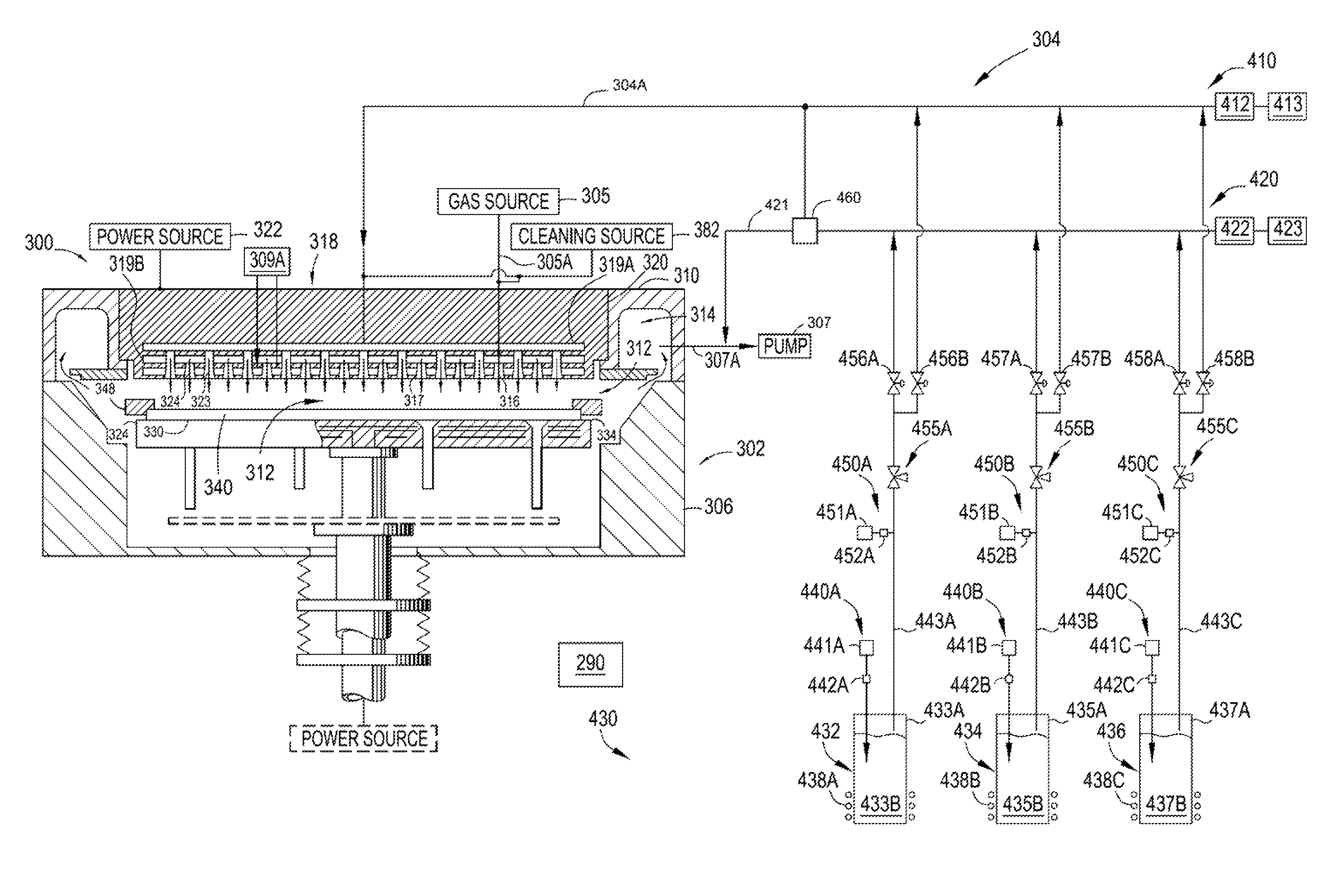
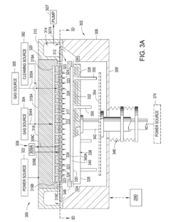
Apparatus and method of forming an indium gallium zinc oxide layer
PatentActiveUS9214340B2
Innovation
- A method and apparatus for forming a multi-element containing film using a gas distribution plate assembly with a precursor plenum and heat exchanging channel, allowing for precise control of precursor gas flow and composition, enabling the deposition of IGZO layers with tailored stoichiometry and reduced environmental exposure.
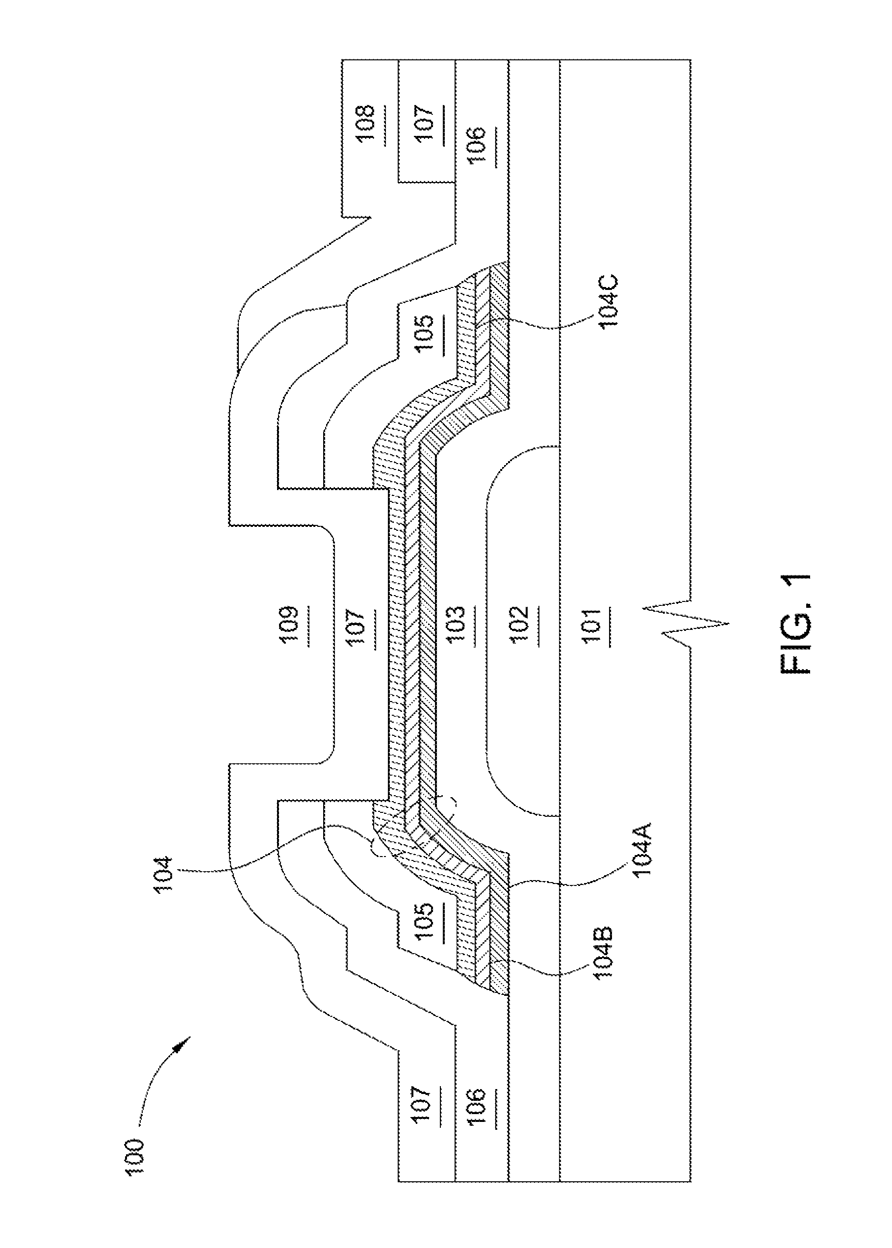

Indium gallium zinc oxide layers for thin film transistors
PatentInactiveUS9502242B2
Innovation
- The use of chemical vapor deposition (CVD) processes for forming IGZO active layers without a prior nucleation layer, combined with in-situ substrate cleaning and preheating, allows for the deposition of high-mobility IGZO layers with controlled stoichiometry and reduced exposure to air, improving throughput and reducing environmental degradation.

Material Supply Chain Analysis for IGZO Production
The IGZO (Indium Gallium Zinc Oxide) material supply chain represents a critical component in the semiconductor and display industries, with significant implications for thin film deposition techniques. The supply chain begins with raw material extraction, where indium presents the most significant challenge due to its scarcity. Global indium reserves are limited, with China controlling approximately 57% of worldwide production, followed by South Korea and Japan. This geographic concentration creates potential supply vulnerabilities for manufacturers outside Asia.
Processing of raw materials into high-purity precursors suitable for IGZO deposition represents another critical supply chain segment. The required 99.9999% purity level necessitates specialized refining capabilities possessed by only a handful of companies globally, including Umicore (Belgium), Indium Corporation (USA), and JX Nippon Mining & Metals (Japan). These companies have established significant barriers to entry through proprietary purification technologies.
Target manufacturing for physical vapor deposition methods constitutes another vital link in the IGZO supply chain. Companies like Materion, Tosoh, and Praxair Surface Technologies dominate this specialized market segment, providing sputtering targets with precise stoichiometric compositions essential for consistent IGZO film properties. The manufacturing of these targets requires sophisticated metallurgical processes and quality control systems.
For chemical vapor deposition approaches, precursor chemicals represent a specialized market dominated by Air Liquide, Merck, and Sigma-Aldrich. These companies have developed proprietary metal-organic compounds specifically optimized for IGZO deposition, with tight specifications for vapor pressure, decomposition temperature, and reactivity profiles.
Supply chain resilience has become increasingly important following recent global disruptions. The COVID-19 pandemic exposed vulnerabilities in the just-in-time inventory systems previously employed throughout the electronics industry. Consequently, major display manufacturers have begun implementing strategic stockpiling of critical materials and developing secondary supplier relationships to mitigate future disruption risks.
Sustainability concerns are also reshaping the IGZO supply chain, with increasing focus on recycling indium from end-of-life products. Companies like Umicore and Dowa Holdings have developed specialized processes to recover indium from LCD panels, potentially creating a circular economy model that could alleviate some supply constraints while reducing environmental impact.
Environmental Impact of IGZO Manufacturing Processes
The manufacturing processes of IGZO (Indium Gallium Zinc Oxide) thin films present significant environmental considerations that warrant thorough examination. The production of these advanced semiconductor materials involves several potentially harmful substances and energy-intensive processes that contribute to environmental degradation if not properly managed.
Primary environmental concerns stem from the use of rare and toxic elements, particularly indium, which is classified as a critical raw material due to its limited global supply and extraction challenges. Mining and processing of indium generates substantial waste and can lead to soil and water contamination. Additionally, the sputtering and chemical vapor deposition techniques commonly employed in IGZO film production require substantial energy inputs, contributing to carbon emissions and climate impact.
Chemical waste management represents another significant environmental challenge. The etching processes utilized in IGZO manufacturing typically involve hazardous acids and solvents that require specialized disposal protocols. Improper handling of these chemicals can result in air pollution and water contamination, posing risks to both ecosystem health and human populations in manufacturing regions.
Water consumption during IGZO production is notably high, particularly in cleaning and cooling processes. A single manufacturing facility may consume millions of gallons annually, placing pressure on local water resources. This aspect becomes increasingly problematic as many electronics manufacturing hubs are located in regions already experiencing water stress.
Recent technological advancements have begun addressing these environmental concerns. Low-temperature deposition techniques have emerged that significantly reduce energy requirements while maintaining film quality. Several leading manufacturers have implemented closed-loop water recycling systems that reduce freshwater consumption by up to 60% compared to conventional approaches.
Material efficiency improvements represent another promising development. Advanced target utilization in sputtering processes has increased material efficiency from approximately 30% to over 70% in state-of-the-art systems, substantially reducing waste generation. Additionally, research into indium-free alternatives and recovery processes from electronic waste shows potential for mitigating supply chain vulnerabilities and environmental impacts associated with raw material extraction.
Regulatory frameworks worldwide are increasingly focusing on the environmental footprint of electronics manufacturing. The European Union's Restriction of Hazardous Substances (RoHS) directive and similar regulations in other regions have prompted manufacturers to develop more environmentally sustainable IGZO production methods, driving innovation in greener deposition technologies and waste management practices.
Unlock deeper insights with Patsnap Eureka Quick Research — get a full tech report to explore trends and direct your research. Try now!
Generate Your Research Report Instantly with AI Agent
Supercharge your innovation with Patsnap Eureka AI Agent Platform!