Comparative Study of IGZO Thin Film Efficiency Across Applications
SEP 28, 20259 MIN READ
Generate Your Research Report Instantly with AI Agent
Patsnap Eureka helps you evaluate technical feasibility & market potential.
IGZO Thin Film Technology Evolution and Objectives
Indium Gallium Zinc Oxide (IGZO) thin film technology represents a significant advancement in semiconductor materials, emerging as a transformative solution for various electronic applications. Since its initial development in the early 2000s by researchers at Tokyo Institute of Technology, IGZO has evolved from an experimental compound to a commercially viable technology. The evolution trajectory has been marked by continuous improvements in electron mobility, stability, and manufacturing processes, enabling its integration into increasingly sophisticated devices.
The fundamental advantage of IGZO lies in its unique electronic structure, combining the benefits of amorphous silicon's uniformity with crystalline silicon's superior electron mobility. This hybrid characteristic has positioned IGZO as an ideal material for applications requiring both high performance and large-area uniformity, particularly in display technologies where traditional silicon-based semiconductors face limitations.
Market adoption of IGZO technology has followed a clear progression pattern, beginning with implementation in small to medium-sized displays before expanding to larger panels and more demanding applications. The technology's evolution has been accelerated by collaborative efforts between academic institutions and industry leaders, resulting in significant patent portfolios and proprietary manufacturing techniques that have shaped the competitive landscape.
Recent technological advancements have focused on enhancing IGZO's electrical stability under various environmental conditions, reducing defect states, and optimizing deposition methods to achieve greater consistency across large substrates. These improvements have directly addressed early challenges related to threshold voltage shifts and performance degradation under prolonged operation.
The primary objective of current IGZO research centers on comparative efficiency analysis across diverse applications, from traditional display technologies to emerging fields such as flexible electronics, transparent circuitry, and medical imaging systems. Understanding performance variations across these applications provides critical insights for future optimization strategies and helps identify the most promising development pathways.
Technical goals for IGZO thin film advancement include achieving electron mobility exceeding 50 cm²/Vs in production environments, reducing power consumption by at least 30% compared to current standards, and developing deposition techniques compatible with temperature-sensitive substrates for flexible electronics applications. Additionally, researchers aim to enhance IGZO's resistance to environmental factors while maintaining its exceptional transparency characteristics.
The evolution of IGZO technology represents a convergence of materials science, electronic engineering, and manufacturing innovation, with each advancement expanding the potential application scope and market value of this versatile semiconductor material.
Market Applications and Demand Analysis for IGZO Technology
The IGZO (Indium Gallium Zinc Oxide) thin film technology market has experienced significant growth over the past decade, primarily driven by its superior performance characteristics in display applications. The global market for IGZO-based products was valued at approximately $2.3 billion in 2022 and is projected to reach $5.7 billion by 2028, representing a compound annual growth rate of 16.4% during the forecast period.
Display technology represents the largest application segment for IGZO thin films, accounting for over 70% of the total market share. Within this segment, the demand is primarily fueled by manufacturers of high-resolution displays for smartphones, tablets, and large-format televisions. The superior electron mobility of IGZO compared to traditional amorphous silicon (a-Si) has made it particularly attractive for high-resolution, low-power display applications.
Consumer electronics giants including Samsung, LG, Sharp, and Apple have incorporated IGZO technology into their premium product lines, signaling strong market confidence. The technology's ability to deliver higher pixel densities while consuming less power has become a critical differentiator in the competitive consumer electronics landscape.
Beyond displays, emerging applications in flexible electronics, transparent electronics, and medical imaging are creating new market opportunities. The flexible electronics segment is expected to grow at the fastest rate, with a projected CAGR of 22.7% through 2028, as manufacturers seek materials compatible with bendable and foldable device architectures.
Regional analysis indicates that Asia-Pacific dominates the IGZO market with approximately 65% share, followed by North America and Europe. Japan and South Korea lead in production capacity, while China is rapidly expanding its manufacturing capabilities to reduce dependency on imports.
Market challenges include the relatively high cost of indium as a raw material and competition from alternative technologies such as LTPS (Low-Temperature Polysilicon). The price volatility of indium, which is classified as a critical material with limited global supply, poses a significant concern for long-term market stability.
Industry surveys indicate that manufacturers are increasingly focused on improving IGZO thin film efficiency across different applications to maximize return on investment. The efficiency variations observed in different application contexts (displays versus sensors versus thin-film transistors) represent both a challenge and an opportunity for material scientists and device engineers to optimize formulations for specific use cases.
Current IGZO Efficiency Status and Technical Barriers
The current efficiency status of IGZO (Indium Gallium Zinc Oxide) thin films varies significantly across different application domains, with several technical barriers impeding further advancement. In display technologies, IGZO thin films have achieved electron mobility values ranging from 10-15 cm²/Vs in commercial applications, which represents a substantial improvement over amorphous silicon (0.5-1 cm²/Vs) but remains below the theoretical potential of the material. Laboratory demonstrations have reported mobility values exceeding 40 cm²/Vs under optimized conditions, highlighting a considerable gap between research achievements and mass production capabilities.
One of the primary technical barriers facing IGZO implementation is the stability issue under prolonged bias stress and environmental factors. Threshold voltage shifts occur during extended operation, particularly under illumination (photo-bias stress) and elevated temperatures, compromising the long-term reliability of devices. This instability stems from charge trapping at the semiconductor-dielectric interface and oxygen vacancy modulation within the IGZO film structure.
Uniformity across large-area substrates presents another significant challenge, especially as display manufacturers push toward larger panel sizes and higher resolutions. The current industrial deposition methods, primarily RF sputtering, struggle to maintain consistent film properties across Gen 10.5 substrates (2940 × 3370 mm), resulting in performance variations that affect yield rates and product quality. Thickness variations as small as 5% can lead to noticeable differences in electrical characteristics across the panel.
Contact resistance at the source/drain interfaces remains problematic, limiting the overall device performance despite improvements in channel mobility. Current metal contact schemes typically result in resistance values of 10⁴-10⁵ Ω·cm, which becomes increasingly significant as device dimensions shrink below 5 μm channel lengths. This parasitic resistance effectively negates the intrinsic mobility advantages of IGZO in highly scaled devices.
For flexible electronics applications, IGZO films face additional challenges related to mechanical durability. While IGZO demonstrates better flexibility than crystalline semiconductors, performance degradation occurs after repeated bending cycles, with typical devices showing 15-20% reduction in mobility after 1,000 bending cycles at 5 mm radius. This limitation restricts applications in wearable technology and foldable displays where more severe deformation is expected.
Power efficiency in IGZO-based circuits also presents ongoing challenges. Although IGZO TFTs offer lower leakage currents compared to silicon alternatives, the relatively high operating voltages (typically 10-15V for robust operation) limit their application in low-power portable devices. Research efforts to reduce operating voltage while maintaining performance reliability have shown promising results in laboratory settings but have yet to translate to commercial manufacturing processes.
Comparative Analysis of Current IGZO Implementation Methods
01 Composition and structure optimization of IGZO thin films
The efficiency of IGZO (Indium Gallium Zinc Oxide) thin films can be improved by optimizing their composition and structure. This includes adjusting the ratio of indium, gallium, and zinc, controlling the oxygen content, and modifying the crystalline structure. These optimizations can enhance carrier mobility, reduce defects, and improve overall electrical performance of the thin film transistors.- Composition and structure optimization of IGZO thin films: The efficiency of IGZO (Indium Gallium Zinc Oxide) thin films can be improved through optimizing their composition and structure. This includes adjusting the ratio of indium, gallium, and zinc, controlling the oxygen content, and optimizing the crystalline structure. These modifications can enhance carrier mobility, reduce defects, and improve overall electrical performance of the thin film transistors (TFTs).
- Deposition techniques for high-efficiency IGZO films: Various deposition methods significantly impact the efficiency of IGZO thin films. Techniques such as sputtering, atomic layer deposition (ALD), pulsed laser deposition (PLD), and solution processing can be optimized to produce high-quality IGZO films with improved uniformity, reduced impurities, and enhanced electrical properties. Process parameters like temperature, pressure, and gas flow rates during deposition play crucial roles in determining film quality.
- Post-deposition treatments to enhance IGZO performance: Post-deposition treatments such as annealing, plasma treatment, and passivation can significantly improve IGZO thin film efficiency. These processes help reduce oxygen vacancies, eliminate trap states, improve interface quality, and enhance stability. Thermal annealing in various atmospheres (oxygen, nitrogen, forming gas) at optimized temperatures can particularly improve carrier mobility and reduce threshold voltage shifts in IGZO-based devices.
- Interface engineering for improved IGZO device performance: The efficiency of IGZO thin film devices is heavily influenced by interface quality between the IGZO layer and adjacent layers (gate dielectric, source/drain contacts, passivation layers). Interface engineering techniques include insertion of buffer layers, surface treatments, and selection of compatible materials to reduce interface traps, contact resistance, and improve charge transport. These approaches minimize carrier scattering and enhance overall device efficiency.
- Novel device architectures utilizing IGZO thin films: Innovative device architectures can maximize the efficiency of IGZO thin films in various applications. These include double-gate structures, vertical channel designs, self-aligned structures, and integration with other semiconductor materials to form heterojunctions. Such novel architectures can enhance channel control, reduce parasitic capacitance, improve switching characteristics, and enable new functionalities in displays, sensors, and other electronic applications.
02 Deposition techniques for high-efficiency IGZO films
Various deposition methods can significantly impact the efficiency of IGZO thin films. Techniques such as sputtering, atomic layer deposition, pulsed laser deposition, and solution processing can be optimized to produce high-quality films with uniform thickness and minimal defects. Process parameters including temperature, pressure, and gas flow rates during deposition play crucial roles in determining the final film properties and device performance.Expand Specific Solutions03 Post-deposition treatments to enhance IGZO performance
Post-deposition treatments such as annealing, plasma treatment, and passivation can significantly improve the efficiency of IGZO thin films. These processes help to reduce oxygen vacancies, improve interface quality, and enhance stability. Thermal annealing in various atmospheres (oxygen, nitrogen, forming gas) can optimize the electrical properties by modifying the film microstructure and reducing defect states.Expand Specific Solutions04 Interface engineering for improved IGZO thin film efficiency
The efficiency of IGZO thin films can be enhanced through interface engineering between the semiconductor and adjacent layers. This includes the development of optimized gate dielectrics, buffer layers, and contact electrodes. Controlling the interface states and reducing charge trapping at boundaries can significantly improve carrier transport properties and device stability, leading to higher overall efficiency.Expand Specific Solutions05 Novel device architectures utilizing IGZO thin films
Innovative device architectures can maximize the efficiency of IGZO thin films in various applications. These include double-gate structures, vertical channel designs, and heterojunction configurations. By optimizing the device geometry, channel dimensions, and integration with other materials, the electrical performance and energy efficiency of IGZO-based devices can be significantly improved for applications in displays, sensors, and flexible electronics.Expand Specific Solutions
Key Patents and Scientific Breakthroughs in IGZO Efficiency
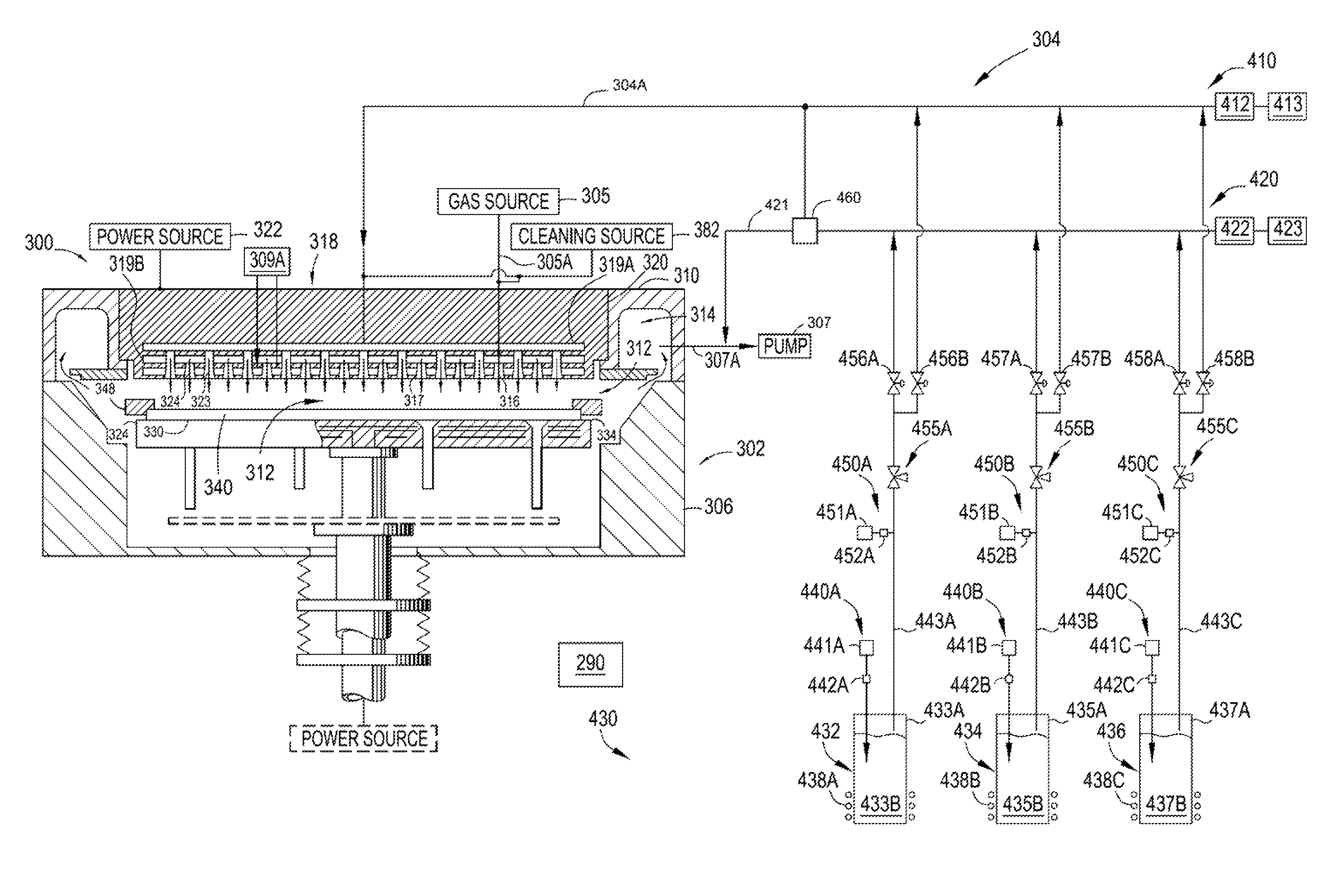
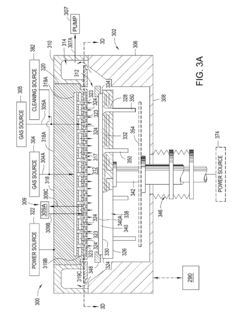
Apparatus and method of forming an indium gallium zinc oxide layer
PatentActiveUS9214340B2
Innovation
- A method and apparatus for forming a multi-element containing film using a gas distribution plate assembly with a precursor plenum and heat exchanging channel, allowing for precise control of precursor gas flow and composition, enabling the deposition of IGZO layers with tailored stoichiometry and reduced environmental exposure.
Manufacturing Process Optimization for IGZO Thin Films
The optimization of manufacturing processes for IGZO (Indium Gallium Zinc Oxide) thin films represents a critical factor in determining their efficiency across various applications. Current manufacturing techniques primarily include sputtering, pulsed laser deposition (PLD), and solution-based methods, each with distinct advantages and limitations affecting film quality and performance characteristics.
RF magnetron sputtering remains the dominant industrial method due to its scalability and uniformity control. Recent advancements have focused on optimizing sputtering parameters, with research indicating that maintaining substrate temperatures between 200-300°C during deposition significantly enhances carrier mobility. Studies by Tokyo Institute of Technology demonstrated that precise oxygen partial pressure control (typically 0.1-0.5 Pa) during sputtering directly correlates with defect density reduction and subsequent performance improvements across display, sensor, and memory applications.
Post-deposition annealing processes have emerged as crucial optimization steps, with thermal annealing in oxygen-rich environments at 300-400°C showing up to 40% improvement in thin film transistor (TFT) stability. Notably, research from Samsung Advanced Institute of Technology revealed that two-step annealing processes—combining vacuum and oxygen environments—can effectively balance carrier concentration and mobility requirements for different application domains.
Atomic layer deposition (ALD) techniques are gaining prominence for ultra-thin IGZO films, offering atomic-level thickness control critical for next-generation flexible electronics. The precise stoichiometric control possible with ALD has demonstrated particular efficiency advantages in transparent photodetector applications, where the In:Ga:Zn ratio significantly impacts photoresponse characteristics.
Solution-based processing methods, including sol-gel and spin-coating techniques, represent cost-effective alternatives showing promise for large-area applications. Recent innovations in precursor chemistry have addressed previous limitations in film uniformity, with metal acetate-based precursors demonstrating improved homogeneity across substrates exceeding 1m² in area.
Interface engineering between IGZO and adjacent layers has proven essential for optimizing device performance. Studies from KAIST and MIT have independently confirmed that introducing nanometer-scale buffer layers can significantly reduce interface trap densities, enhancing carrier transport efficiency particularly in memory and sensor applications where interface phenomena dominate performance metrics.
Emerging manufacturing innovations include high-pressure annealing techniques and plasma-enhanced processing, both showing potential for reducing processing temperatures while maintaining or improving film quality—a critical consideration for integration with temperature-sensitive substrates in flexible electronics applications.
Environmental Impact and Sustainability of IGZO Technology
The environmental impact of IGZO (Indium Gallium Zinc Oxide) technology represents a critical consideration in its widespread adoption across various applications. IGZO thin films offer significant sustainability advantages compared to conventional semiconductor materials, primarily through reduced energy consumption during both manufacturing and operation. The production process of IGZO typically requires lower temperatures than traditional silicon-based semiconductors, resulting in approximately 30-40% less energy consumption during fabrication.
When implemented in display technologies, IGZO thin films demonstrate remarkable power efficiency, reducing device energy consumption by up to 80% compared to amorphous silicon alternatives. This efficiency stems from IGZO's superior electron mobility and lower leakage current, enabling displays to maintain images with minimal power input. The extended battery life in portable devices directly translates to reduced charging frequency and lower lifetime carbon footprints.
Material resource considerations present both challenges and opportunities for IGZO sustainability. Indium, a key component, faces supply constraints as a relatively rare element, with primary sources concentrated in China, South Korea, and Japan. Current global reserves are estimated at approximately 15,000 tons, raising concerns about long-term availability. However, emerging recycling technologies show promise in recovering up to 90% of indium from end-of-life electronics, potentially creating a more sustainable material cycle.
The manufacturing process for IGZO thin films produces fewer toxic byproducts compared to conventional semiconductor fabrication. Specifically, IGZO production generates approximately 40% less hazardous waste and requires fewer harsh chemicals for etching and cleaning processes. This reduction in harmful emissions and waste contributes significantly to the overall environmental profile of IGZO-based devices.
Life cycle assessments indicate that IGZO-enabled devices maintain environmental advantages throughout their operational lifespan. The extended durability of IGZO thin films, with demonstrated stability over 10,000+ hours of continuous operation, reduces replacement frequency and associated electronic waste. Furthermore, the material's compatibility with flexible substrates enables thinner, more resource-efficient device designs that require less packaging material.
Future sustainability improvements for IGZO technology are focusing on alternative material compositions that reduce dependence on rare elements while maintaining performance characteristics. Research into zinc-tin oxide and other alternative transparent semiconductors shows promise for addressing resource constraints while preserving the environmental benefits that make IGZO an attractive technology across diverse applications.
Unlock deeper insights with Patsnap Eureka Quick Research — get a full tech report to explore trends and direct your research. Try now!
Generate Your Research Report Instantly with AI Agent
Supercharge your innovation with Patsnap Eureka AI Agent Platform!