How Nano-Imprint Lithography relates to Vacuum Forming Advancements
JUL 30, 20259 MIN READ
Generate Your Research Report Instantly with AI Agent
Patsnap Eureka helps you evaluate technical feasibility & market potential.
NIL and VF Background
Nano-Imprint Lithography (NIL) and Vacuum Forming (VF) are two distinct manufacturing processes that have evolved significantly over the past few decades. NIL, a relatively newer technology, emerged in the 1990s as a promising method for high-resolution patterning at the nanoscale. It was developed to overcome the limitations of traditional photolithography techniques in achieving ever-smaller feature sizes in semiconductor manufacturing.
VF, on the other hand, has a longer history dating back to the 1950s. It was initially developed as a cost-effective method for producing three-dimensional plastic parts, particularly in the packaging and automotive industries. The process involves heating a thermoplastic sheet and using vacuum pressure to conform it to a mold, creating complex shapes and textures.
The evolution of NIL has been driven by the increasing demand for smaller, more efficient electronic devices. As Moore's Law pushed the boundaries of conventional lithography, NIL offered a potential solution for creating nanoscale patterns with high fidelity and throughput. The technology has progressed from simple thermal imprinting to more advanced techniques like UV-NIL and Roll-to-Roll NIL, enabling broader applications in areas such as photonics, biotechnology, and energy storage.
VF has also seen significant advancements, particularly in terms of precision and material capabilities. Modern VF processes incorporate computer-controlled heating and cooling systems, advanced mold designs, and a wider range of compatible materials. These improvements have expanded VF's applications beyond traditional plastics to include advanced composites and even some metallic materials.
The intersection of NIL and VF technologies represents an exciting frontier in advanced manufacturing. While they originated in different industries and operate at vastly different scales, both processes share fundamental principles of material deformation and pattern transfer. Recent research has explored the potential of combining NIL's high-resolution patterning capabilities with VF's ability to create large-scale, three-dimensional structures.
This convergence has led to innovative applications in fields such as flexible electronics, where large-area, nanopatterned surfaces are required. For instance, researchers have investigated using NIL techniques to create nanoscale textures on polymer sheets, which are then shaped using modified VF processes. This approach could enable the mass production of complex, functional surfaces with both micro and nanoscale features.
As both technologies continue to evolve, their synergies are likely to yield new manufacturing paradigms. The integration of NIL principles into VF processes could lead to more precise control over surface properties at multiple scales, opening up possibilities for advanced materials with tailored optical, mechanical, or biological properties. This convergence exemplifies the broader trend in advanced manufacturing towards multi-scale, multi-functional production techniques.
Market Demand Analysis
The market demand for Nano-Imprint Lithography (NIL) and its relation to vacuum forming advancements has been steadily growing in recent years. This growth is primarily driven by the increasing need for high-resolution, cost-effective patterning techniques in various industries, including semiconductor manufacturing, optics, and biotechnology.
In the semiconductor industry, NIL has gained significant traction as a potential alternative to traditional photolithography techniques. As the demand for smaller, more powerful electronic devices continues to rise, manufacturers are seeking innovative methods to produce nanoscale features at lower costs. NIL offers the ability to create patterns with resolutions below 10 nanometers, making it an attractive option for next-generation semiconductor production.
The optics and photonics sector has also shown a growing interest in NIL technology. The ability to create precise, nanoscale structures is crucial for developing advanced optical components, such as diffractive optical elements, waveguides, and photonic crystals. This has led to an increased demand for NIL equipment and materials in the optics industry.
Biotechnology and life sciences represent another significant market for NIL applications. The technology enables the creation of nanostructured surfaces for cell culture, biosensors, and microfluidic devices. As research in these fields intensifies, the demand for NIL-based solutions is expected to grow substantially.
The relationship between NIL and vacuum forming advancements has further expanded the market potential for both technologies. Vacuum forming, traditionally used in packaging and product manufacturing, has benefited from the precision and scalability offered by NIL. This synergy has opened up new possibilities in areas such as flexible electronics, wearable devices, and advanced packaging solutions.
The automotive industry has also shown interest in NIL and vacuum forming advancements for creating lightweight, high-performance components. The ability to produce complex, nanoscale patterns on large surfaces has potential applications in areas such as aerodynamics, fuel efficiency, and smart coatings.
As environmental concerns continue to grow, there is an increasing demand for sustainable manufacturing processes. NIL, when combined with vacuum forming techniques, offers the potential for more energy-efficient and material-conserving production methods. This aligns well with the global trend towards greener technologies and circular economy principles.
The market for NIL and related vacuum forming technologies is expected to expand further as research and development efforts continue to improve the scalability, reliability, and cost-effectiveness of these processes. This growth is likely to be driven by emerging applications in fields such as quantum computing, advanced materials, and nanotechnology-enabled consumer products.
Technical Challenges
Nano-Imprint Lithography (NIL) and Vacuum Forming are both advanced manufacturing techniques, but they face distinct technical challenges in their application to semiconductor and packaging industries respectively. The integration of these technologies presents unique obstacles that researchers and engineers are actively working to overcome.
One of the primary challenges in NIL is achieving high-resolution patterns over large areas consistently. While NIL can produce features at the nanoscale, maintaining uniformity across a full wafer remains difficult. This is particularly problematic when attempting to scale up production for commercial applications. The issue is compounded by the need for precise alignment between multiple imprint steps, which becomes increasingly challenging as feature sizes decrease.
Material selection poses another significant hurdle for NIL. The resist materials used must possess specific properties, including low viscosity for easy filling of mold features, rapid curing under UV exposure, and sufficient mechanical strength to maintain pattern integrity after demolding. Developing resists that meet all these criteria while also being compatible with subsequent processing steps is an ongoing area of research.
In the realm of Vacuum Forming, a major challenge lies in achieving high-precision molding for complex geometries. While the technique is well-established for larger-scale products, adapting it for micro- and nano-scale features requires significant advancements in mold design and process control. The vacuum pressure distribution must be carefully managed to ensure uniform material draw across intricate patterns.
Temperature control presents another critical challenge in both NIL and Vacuum Forming. For NIL, maintaining precise temperature during the imprinting process is crucial for achieving consistent results. In Vacuum Forming, temperature gradients can lead to uneven material distribution and warping, particularly when working with thin films or advanced polymers.
The integration of NIL principles into Vacuum Forming processes introduces additional complexities. Combining the high-resolution capabilities of NIL with the large-area processing of Vacuum Forming requires innovative approaches to mold design, material handling, and process automation. Achieving this integration while maintaining cost-effectiveness and high throughput remains a significant technical challenge.
Contamination control is another shared concern between NIL and Vacuum Forming. In NIL, even microscopic particles can disrupt pattern transfer, leading to defects. For Vacuum Forming, especially when targeting high-precision applications, cleanliness of the forming environment and materials is crucial to prevent surface imperfections.
As both technologies advance, there is a growing need for in-line metrology and quality control systems capable of detecting nanoscale defects at production speeds. Developing such systems that can operate reliably in manufacturing environments without slowing down production is a significant technical challenge that spans both NIL and advanced Vacuum Forming applications.
Current NIL-VF Solutions
01 Imprint mold design and fabrication
Nano-imprint lithography relies heavily on the design and fabrication of high-quality imprint molds. These molds are typically made from materials like quartz or silicon and feature nanoscale patterns that are transferred to the substrate. Advanced techniques are used to create precise and durable molds, including electron beam lithography and focused ion beam milling.- Imprint mold design and fabrication: Nano-imprint lithography relies heavily on the design and fabrication of high-quality imprint molds. These molds are typically made from materials like quartz or silicon and feature nanoscale patterns that are transferred to the substrate. Advanced techniques are used to create precise and durable molds, including electron beam lithography and focused ion beam milling.
- Resist materials and formulations: The development of specialized resist materials is crucial for nano-imprint lithography. These materials need to have specific properties such as low viscosity for easy filling of mold features, rapid curing under UV light or heat, and good etch resistance. Researchers are continually working on new resist formulations to improve resolution, reduce defects, and enhance overall performance.
- Imprinting process optimization: Optimizing the imprinting process is essential for achieving high-quality, high-throughput nano-imprint lithography. This includes controlling parameters such as pressure, temperature, and curing time. Advanced techniques like step-and-repeat imprinting and roll-to-roll processes are being developed to increase efficiency and enable large-area patterning.
- Defect reduction and pattern transfer: Minimizing defects and ensuring accurate pattern transfer are ongoing challenges in nano-imprint lithography. Researchers are developing methods to reduce bubble formation, improve mold-substrate alignment, and enhance the fidelity of pattern transfer. This includes the use of advanced metrology tools and the development of novel etching techniques to transfer imprinted patterns into underlying layers.
- Integration with other technologies: Nano-imprint lithography is being integrated with other advanced manufacturing technologies to expand its capabilities. This includes combining it with directed self-assembly processes, incorporating it into 3D printing systems, and developing hybrid lithography approaches that combine nano-imprint with other patterning techniques. These integrations aim to overcome limitations and enable new applications in fields such as electronics, photonics, and biotechnology.
02 Resist materials and formulations
The development of specialized resist materials is crucial for nano-imprint lithography. These materials need to have specific properties such as low viscosity for easy filling of mold features, rapid curing under UV light or heat, and good etch resistance. Researchers are continuously working on new resist formulations to improve resolution, reduce defects, and enhance overall performance.Expand Specific Solutions03 Imprinting process optimization
Optimizing the imprinting process is essential for achieving high-quality nanostructures. This includes controlling parameters such as pressure, temperature, and curing time. Advanced techniques like step-and-repeat imprinting and roll-to-roll imprinting are being developed to increase throughput and enable large-area patterning for industrial applications.Expand Specific Solutions04 Defect reduction and pattern transfer
Minimizing defects and ensuring accurate pattern transfer are ongoing challenges in nano-imprint lithography. Researchers are developing techniques to reduce issues such as bubble formation, incomplete filling, and residual layer thickness variations. Additionally, methods for improving the fidelity of pattern transfer from the imprinted resist to the underlying substrate are being investigated.Expand Specific Solutions05 Integration with other nanofabrication techniques
Nano-imprint lithography is being integrated with other nanofabrication techniques to create more complex and functional nanostructures. This includes combining imprinting with processes like etching, deposition, and lift-off. Hybrid approaches that incorporate elements of both optical and imprint lithography are also being explored to leverage the strengths of each technique.Expand Specific Solutions
Key Industry Players
The competition landscape for Nano-Imprint Lithography (NIL) in relation to Vacuum Forming Advancements is characterized by a mature market with significant growth potential. The industry is in a phase of technological refinement, with key players like Molecular Imprints, Canon, and FUJIFILM leading innovation. Market size is expanding due to increasing demand in semiconductor and display manufacturing. Technological maturity varies, with companies like Canon Nanotechnologies and EV Group pushing boundaries in high-resolution patterning. Universities such as Nanjing University and Wuhan University contribute to fundamental research, while industry collaborations with entities like Western Digital and Toshiba drive practical applications.
Molecular Imprints, Inc.
Technical Solution: Molecular Imprints has developed a proprietary Jet and Flash Imprint Lithography (J-FIL) technology, which combines nano-imprint lithography with vacuum forming advancements. Their process uses a low-viscosity resist that is dispensed in droplets onto the substrate, followed by imprinting with a patterned template under vacuum conditions. This approach allows for high-resolution patterning down to sub-10nm features[1]. The vacuum environment during imprinting helps eliminate air bubbles and ensures uniform filling of template features. Additionally, they have integrated their technology with step-and-repeat systems, enabling large-area patterning for semiconductor and display applications[2].
Strengths: High-resolution patterning capability, large-area compatibility, and reduced defectivity due to vacuum-assisted imprinting. Weaknesses: May require specialized equipment and materials, potentially higher cost compared to traditional lithography methods.
Canon, Inc.
Technical Solution: Canon has developed a nanoimprint lithography system that incorporates vacuum forming techniques to enhance pattern transfer accuracy. Their approach utilizes a flexible mold made of a gas-permeable material, which is pressed against a resist-coated substrate under vacuum conditions. This allows for the evacuation of air from the mold-resist interface, preventing bubble formation and ensuring uniform contact[3]. Canon's system also employs a UV-curable resist that is optimized for low viscosity and rapid curing, enabling high-throughput production. The company has demonstrated the ability to pattern features as small as 15nm over large areas, making it suitable for next-generation semiconductor and display manufacturing[4].
Strengths: High-resolution patterning, large-area compatibility, and improved pattern transfer accuracy due to vacuum-assisted molding. Weaknesses: May require specialized mold materials and resist formulations, potentially limiting flexibility in material choices.
Core NIL-VF Innovations
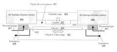
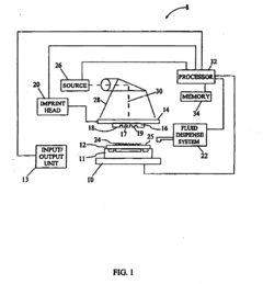
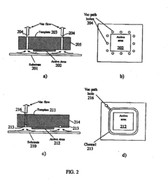
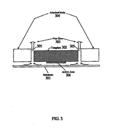
Partial vacuum environment imprinting
PatentActiveUS7462028B2
Innovation
- The implementation of a partial vacuum environment created using channels or holes in the template, which induces a uniform partial vacuum and allows for the use of process gases like helium, while also utilizing additional plates or air bearings to maintain a controlled pressure and reduce separation forces during the imprinting process.
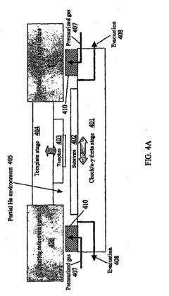
Lithography imprinting system
PatentActiveEP2001602B1
Innovation
- The implementation of a partial vacuum environment during the nanolithography imprinting process, utilizing a template with specific geometries and gas management systems to create a controlled atmosphere, reduces fill time, defects, and separation forces, enhancing the efficiency of the imprinting process.
Material Advancements
The advancements in materials science have played a crucial role in the development and refinement of both Nano-Imprint Lithography (NIL) and Vacuum Forming technologies. These material innovations have significantly enhanced the capabilities and applications of both processes, particularly in the realm of nanoscale fabrication and large-scale manufacturing.
In the context of NIL, the development of novel resist materials has been a key factor in improving the resolution and fidelity of nanoscale patterns. High-performance resist materials with enhanced mechanical properties, such as increased hardness and reduced shrinkage, have enabled the creation of more precise and stable nanostructures. Additionally, the introduction of UV-curable resists has facilitated faster processing times and improved throughput in NIL applications.
The evolution of mold materials has also been instrumental in advancing NIL technology. Silicon-based molds have been largely replaced by more durable and flexible alternatives, such as nickel and polymer-based materials. These new mold materials offer improved longevity, reduced defect rates, and the ability to create more complex three-dimensional nanostructures.
For Vacuum Forming, material advancements have focused on enhancing the performance and versatility of thermoplastic sheets. The development of high-performance polymers with improved thermal stability, impact resistance, and optical clarity has expanded the range of applications for vacuum-formed products. Moreover, the introduction of multi-layer and composite materials has enabled the creation of vacuum-formed components with tailored properties, such as enhanced barrier performance or specific surface characteristics.
The convergence of NIL and Vacuum Forming technologies has been facilitated by advancements in hybrid materials that combine the benefits of both nanoscale patterning and large-scale forming. For instance, the development of nanocomposite materials that can be patterned at the nanoscale using NIL and subsequently shaped through vacuum forming has opened up new possibilities for creating functional surfaces with both micro and macro-scale features.
Furthermore, the progress in anti-sticking coatings and release agents has been crucial for both NIL and Vacuum Forming processes. These materials have significantly improved the demolding process, reducing defects and enhancing the overall quality of the final products. The development of environmentally friendly and biocompatible release agents has also expanded the potential applications of these technologies in sectors such as medical device manufacturing and food packaging.
Environmental Impact
The environmental impact of Nano-Imprint Lithography (NIL) and its relation to vacuum forming advancements is a crucial aspect to consider in the development and implementation of these technologies. NIL, as a high-resolution patterning technique, offers significant advantages in terms of energy efficiency and material consumption compared to traditional lithography methods. This translates to a reduced carbon footprint and less waste generation in the manufacturing process.
Vacuum forming, when combined with NIL techniques, further enhances the environmental benefits. The integration of these technologies allows for more precise and efficient production of complex structures, minimizing material waste and energy consumption. This synergy results in a more sustainable manufacturing process, aligning with global efforts to reduce industrial environmental impact.
One of the key environmental advantages of NIL in relation to vacuum forming is the reduction in chemical usage. Traditional lithography often requires harsh chemicals and solvents, which can have detrimental effects on the environment. NIL, especially when used in conjunction with vacuum forming, significantly reduces the need for these chemicals, leading to cleaner production processes and fewer hazardous waste products.
The precision of NIL also contributes to improved product quality and longevity. When applied to vacuum-formed products, it enables the creation of more durable and functional items. This increased product lifespan reduces the frequency of replacements, ultimately decreasing the overall environmental impact associated with product lifecycle and disposal.
Furthermore, the scalability of NIL and its compatibility with vacuum forming processes opens up possibilities for more localized production. This can lead to reduced transportation needs and associated carbon emissions, as products can be manufactured closer to their point of use. The ability to produce high-quality, complex structures locally aligns with the growing trend towards more sustainable and resilient supply chains.
However, it's important to note that the environmental benefits of these technologies are not without challenges. The production of specialized equipment and materials for NIL and advanced vacuum forming can have its own environmental footprint. Additionally, the disposal or recycling of products created through these processes may present new challenges that need to be addressed to ensure a truly sustainable lifecycle.
In conclusion, the relationship between NIL and vacuum forming advancements presents a promising path towards more environmentally friendly manufacturing processes. By reducing material waste, energy consumption, and chemical usage, while improving product quality and enabling localized production, these technologies contribute to a more sustainable industrial landscape. As research and development in this field continue, further improvements in environmental performance can be expected, potentially revolutionizing manufacturing practices across various industries.
Unlock deeper insights with Patsnap Eureka Quick Research — get a full tech report to explore trends and direct your research. Try now!
Generate Your Research Report Instantly with AI Agent
Supercharge your innovation with Patsnap Eureka AI Agent Platform!