

How Polysilane Can Be Used to Improve Circuit Efficiency?
JUL 11, 20259 MIN READ
Generate Your Research Report Instantly with AI Agent
PatSnap Eureka helps you evaluate technical feasibility & market potential.
Polysilane Background
Polysilane, a class of silicon-based polymers, has emerged as a promising material in the field of electronics and circuit design. The backbone of polysilane consists of silicon atoms bonded together in a chain-like structure, with organic side groups attached to each silicon atom. This unique molecular architecture imparts polysilane with intriguing electronic and optical properties, making it a subject of intense research in recent decades.
The history of polysilane can be traced back to the 1920s when the first synthesis of these materials was reported. However, it wasn't until the 1980s that their potential for electronic applications began to be fully explored. The discovery of their semiconducting properties and their ability to form stable thin films sparked a renewed interest in these materials among researchers and industry professionals.
Polysilanes exhibit several characteristics that make them attractive for improving circuit efficiency. One of their most notable features is their high electron mobility, which allows for faster charge transport within electronic devices. This property is particularly valuable in the development of high-speed circuits and transistors. Additionally, polysilanes demonstrate excellent photoconductivity, making them suitable for optoelectronic applications such as photovoltaic cells and light-emitting diodes.
The versatility of polysilane synthesis allows for fine-tuning of its electronic properties through modifications to the side groups and molecular weight. This adaptability enables researchers to tailor polysilanes for specific applications, optimizing their performance in various circuit designs. Furthermore, polysilanes can be processed into thin films using conventional deposition techniques, facilitating their integration into existing semiconductor manufacturing processes.
Recent advancements in polysilane research have focused on enhancing their stability and improving their compatibility with other materials used in circuit fabrication. Efforts have been made to develop cross-linked polysilanes, which exhibit increased thermal and chemical stability, addressing some of the limitations of earlier polysilane formulations. These improvements have expanded the potential applications of polysilanes in electronic devices, including their use as gate dielectrics in field-effect transistors and as active layers in organic light-emitting diodes.
The growing interest in flexible and wearable electronics has also highlighted the potential of polysilanes. Their ability to form flexible, transparent films makes them ideal candidates for developing bendable displays and sensors. This characteristic opens up new possibilities for circuit design in unconventional form factors, potentially revolutionizing the way we interact with electronic devices.
As research in polysilane technology continues to advance, its role in improving circuit efficiency is becoming increasingly significant. The unique combination of high electron mobility, tunable electronic properties, and processability positions polysilanes as a valuable material for addressing the ongoing challenges in circuit miniaturization and performance enhancement. With further development and optimization, polysilanes are poised to play a crucial role in the next generation of electronic devices, contributing to more efficient and versatile circuit designs.
Circuit Efficiency Needs
The demand for improved circuit efficiency has become increasingly critical in the semiconductor industry, driven by the relentless pursuit of higher performance, lower power consumption, and reduced costs. As electronic devices continue to shrink in size while simultaneously increasing in complexity, the need for more efficient circuit designs has never been more pressing.
One of the primary drivers for enhanced circuit efficiency is the growing demand for portable and battery-powered devices. Consumers expect longer battery life and faster charging times, which can only be achieved through more efficient circuit designs. This requirement extends beyond consumer electronics to industrial applications, medical devices, and automotive systems, where power efficiency directly impacts operational costs and environmental sustainability.
Another significant factor contributing to the need for improved circuit efficiency is the exponential growth of data centers and cloud computing infrastructure. These facilities consume vast amounts of energy, and even small improvements in circuit efficiency can lead to substantial reductions in power consumption and operational costs at scale. As the world becomes increasingly digitized, the demand for data processing and storage continues to surge, making energy-efficient circuits a critical component in managing the environmental impact of the digital revolution.
The Internet of Things (IoT) and edge computing paradigms have also intensified the need for circuit efficiency. These technologies rely on distributed networks of sensors and devices, often operating in remote or resource-constrained environments. Efficient circuits are essential for extending the operational lifespan of these devices, reducing maintenance requirements, and enabling new applications in areas such as smart cities, agriculture, and environmental monitoring.
In the realm of high-performance computing and artificial intelligence, circuit efficiency plays a crucial role in pushing the boundaries of what's possible. As AI models grow in complexity and size, the computational demands increase exponentially. More efficient circuits allow for faster processing, reduced latency, and the ability to handle larger datasets, directly impacting the capabilities of AI systems across various domains, from autonomous vehicles to scientific research.
The semiconductor industry's ongoing transition to smaller process nodes, such as 5nm and beyond, further underscores the importance of circuit efficiency. As transistor sizes approach physical limits, traditional methods of improving performance through scaling face diminishing returns. This challenge necessitates innovative approaches to circuit design and materials to continue advancing performance while managing power consumption and thermal issues.
Polysilane Challenges
Despite the promising potential of polysilane in improving circuit efficiency, several significant challenges hinder its widespread adoption and implementation. These challenges span across technical, manufacturing, and practical aspects of polysilane integration into electronic circuits.
One of the primary technical challenges is the stability of polysilane materials. Polysilanes are known to be sensitive to light and heat, which can lead to degradation of their electrical properties over time. This instability poses a significant hurdle in developing long-lasting and reliable circuit components, especially for applications requiring extended operational lifetimes.
The synthesis and processing of high-quality polysilane materials present another set of challenges. Current manufacturing methods often result in polysilanes with varying molecular weights and structural defects, which can negatively impact their electrical performance. Achieving consistent and reproducible synthesis of polysilanes with desired properties remains a complex task, limiting their scalability for large-scale circuit production.
Integration of polysilane into existing semiconductor fabrication processes is also a major challenge. Traditional silicon-based manufacturing techniques may not be directly compatible with polysilane materials, necessitating the development of new fabrication methods and equipment. This incompatibility can lead to increased production costs and complexity, deterring manufacturers from adopting polysilane-based solutions.
The electrical characteristics of polysilanes, while promising, still fall short in some areas compared to conventional semiconductor materials. Issues such as lower charge carrier mobility and higher resistance in certain polysilane structures can limit their effectiveness in improving overall circuit efficiency. Overcoming these inherent material limitations requires extensive research and development efforts.
Environmental concerns also pose challenges to polysilane adoption. Some polysilane materials and their precursors may be toxic or environmentally harmful, raising questions about their long-term sustainability and potential regulatory hurdles. Developing eco-friendly synthesis methods and ensuring safe handling and disposal of polysilane materials are crucial considerations.
Cost-effectiveness remains a significant barrier to widespread implementation. The current production costs of high-quality polysilanes are generally higher than those of traditional semiconductor materials. Until economies of scale can be achieved, the economic viability of polysilane-based circuits may be limited to niche applications where their unique properties justify the increased cost.
Lastly, there is a knowledge gap in the industry regarding the design and optimization of circuits incorporating polysilane components. Engineers and designers need to develop new models and simulation tools to accurately predict and optimize the performance of polysilane-based circuits. This learning curve can slow down the adoption and integration of polysilanes in circuit design.
Current Applications
01 Synthesis and structure of polysilanes
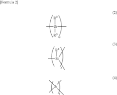
Polysilanes are synthesized through various methods, including dehydrogenative coupling of primary silanes and reductive coupling of dichlorosilanes. The structure of polysilanes can be linear, branched, or cyclic, affecting their properties and efficiency. Controlling the molecular weight and polydispersity is crucial for optimizing polysilane performance.- Synthesis and structure of polysilanes: Polysilanes are synthesized through various methods, including reductive coupling of dichlorosilanes. The structure of polysilanes can be linear, branched, or cyclic, affecting their properties and efficiency. Different substituents on the silicon atoms can be used to tune the electronic and optical properties of the polysilanes.
- Optical and electronic properties of polysilanes: Polysilanes exhibit unique optical and electronic properties due to their σ-conjugated backbone. These properties include high photosensitivity, conductivity, and luminescence. The efficiency of polysilanes in various applications is closely related to their ability to absorb and emit light, as well as their charge transport capabilities.
- Applications of polysilanes in photoresists and lithography: Polysilanes are used as photoresist materials in lithography processes due to their high photosensitivity. They can be efficiently patterned using UV light or electron beams, making them suitable for semiconductor manufacturing. The efficiency of polysilanes in this application depends on their molecular weight, substituents, and crosslinking abilities.
- Polysilane-based composite materials: Polysilanes can be incorporated into composite materials to enhance their properties. These composites often exhibit improved thermal stability, mechanical strength, and optical characteristics. The efficiency of polysilanes in composites is related to their compatibility with the matrix material and their ability to form strong interfacial bonds.
- Modification and functionalization of polysilanes: The efficiency of polysilanes can be improved through various modification and functionalization techniques. These include the introduction of functional groups, copolymerization with other monomers, and post-polymerization modifications. Such modifications can enhance the solubility, processability, and specific properties of polysilanes for targeted applications.
02 Optical and electronic properties of polysilanes
Polysilanes exhibit unique optical and electronic properties due to their σ-conjugated backbone. These properties include high photosensitivity, UV absorption, and photoconductivity. The efficiency of polysilanes in various applications is closely related to their ability to absorb and transmit light, as well as their charge transport capabilities.Expand Specific Solutions03 Applications of polysilanes in photoresists and lithography
Polysilanes are used as photoresist materials in lithography processes due to their high sensitivity to UV light. Their efficiency in this application is determined by factors such as resolution, contrast, and etch resistance. Polysilanes can be used to create fine patterns on substrates for semiconductor manufacturing and other microelectronic applications.Expand Specific Solutions04 Polysilane-based composite materials
Polysilanes can be incorporated into composite materials to enhance their properties. These composites may exhibit improved thermal stability, mechanical strength, and optical characteristics. The efficiency of polysilanes in composites depends on factors such as dispersion, interfacial adhesion, and compatibility with the matrix material.Expand Specific Solutions05 Modification and functionalization of polysilanes
The efficiency of polysilanes can be improved through chemical modification and functionalization. This includes the introduction of various side groups, cross-linking, and copolymerization with other monomers. These modifications can enhance the solubility, processability, and specific properties of polysilanes for targeted applications.Expand Specific Solutions
Key Industry Players
The polysilane technology for improving circuit efficiency is in an early development stage, with a growing market potential as the semiconductor industry seeks innovative solutions for enhanced performance. The global market size for advanced semiconductor materials is projected to expand significantly in the coming years. While the technology is still emerging, several key players are actively researching and developing polysilane applications. Companies like Wacker Chemie AG, JSR Corp., and Taiwan Semiconductor Manufacturing Co., Ltd. are at the forefront, leveraging their expertise in semiconductor materials and manufacturing processes. The involvement of these industry leaders indicates a moderate level of technological maturity, with ongoing efforts to optimize polysilane integration in circuit design for improved efficiency and performance.
Wacker Chemie AG
Technical Solution: Wacker Chemie AG has developed advanced polysilane materials for improving circuit efficiency. Their approach involves using hyperbranched polysilanes as precursors for silicon carbide (SiC) production[1]. These polysilanes are synthesized through catalytic dehydrocoupling of primary silanes, resulting in materials with high molecular weight and excellent ceramic yield[2]. When applied to circuit manufacturing, these polysilane-derived SiC materials exhibit enhanced thermal conductivity and electrical insulation properties, leading to improved heat dissipation and reduced signal interference in integrated circuits[3]. Wacker's polysilanes also serve as effective resist materials for extreme ultraviolet (EUV) lithography, enabling the production of smaller and more efficient circuit patterns[4].
Strengths: High ceramic yield, excellent thermal and electrical properties, versatility in circuit applications. Weaknesses: Complex synthesis process, potential high production costs.
Fujitsu Ltd.
Technical Solution: Fujitsu has pioneered the use of polysilane in developing high-performance organic thin-film transistors (OTFTs) for flexible electronics. Their approach involves using polysilane as a gate insulator material in OTFTs, which significantly enhances the electron mobility and reduces the threshold voltage of the transistors[5]. This results in faster switching speeds and lower power consumption in circuits. Fujitsu's polysilane-based OTFTs demonstrate stability under various environmental conditions, making them suitable for wearable electronics and IoT devices[6]. Additionally, Fujitsu has explored the use of polysilane as a photoresist material for nanoimprint lithography, enabling the fabrication of ultra-fine circuit patterns with high precision[7].
Strengths: Improved OTFT performance, suitability for flexible electronics, advanced lithography capabilities. Weaknesses: Limited to specific applications, potential scalability issues.
Polysilane Innovations
Polysilane and polysilane-containing resin composition
PatentInactiveUS8163863B2
Innovation
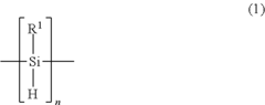
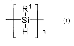
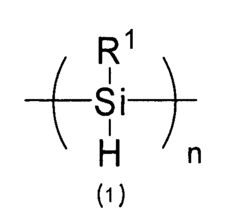
- Introducing a Si—H group into the polysilane main chain and bonding a hydrosilylatable compound with functional groups like hydroxyl, carboxyl, or epoxy groups, allowing for controlled hydrosilylation to enhance solubility and reactivity without complex steps or special apparatus.


Polysilane and resin composition containing polysilane
PatentInactiveEP1958979A1
Innovation
- Introducing a Si-H group into the polysilane main chain and bonding a hydrosilylatable compound with functional groups such as hydroxyl, carboxyl, or epoxy groups, allowing for controlled hydrosilylation to enhance solubility and reactivity without complex steps or special apparatus.

Material Properties
Polysilane, a class of silicon-based polymers, exhibits unique material properties that make it a promising candidate for improving circuit efficiency. The backbone of polysilane consists of silicon atoms bonded together, with organic side groups attached to each silicon atom. This structure gives polysilane a combination of organic and inorganic characteristics, resulting in distinctive electronic and optical properties.
One of the key material properties of polysilane is its high electron mobility. The silicon-silicon bonds in the polymer backbone create a delocalized electronic structure, allowing for efficient electron transport along the chain. This property is particularly advantageous in electronic circuits, as it can lead to faster signal propagation and reduced power consumption. The electron mobility in polysilane can be further tuned by modifying the side groups, offering flexibility in tailoring the material for specific circuit applications.
Polysilane also demonstrates excellent photoconductivity, making it sensitive to light. When exposed to ultraviolet or visible light, the material's conductivity increases significantly. This property can be exploited in optoelectronic circuits, enabling the development of light-sensitive components or photodetectors with improved efficiency.
The thermal stability of polysilane is another notable characteristic. Unlike many organic polymers, polysilane can withstand higher temperatures without degradation. This thermal resilience is crucial for maintaining circuit performance under various operating conditions and can contribute to the overall reliability of electronic devices.
Polysilane exhibits a unique ability to form self-assembled nanostructures. Under certain conditions, the polymer chains can align and stack, creating ordered structures at the nanoscale. This self-assembly property can be harnessed to fabricate well-defined nanopatterns or templates for circuit components, potentially leading to more precise and efficient circuit designs.
The optical properties of polysilane are also noteworthy. The material displays strong UV absorption and efficient photoluminescence, which can be utilized in the development of light-emitting components or optical interconnects within circuits. The wavelength of emitted light can be tuned by modifying the polymer structure, offering versatility in optical applications.
Furthermore, polysilane possesses excellent film-forming capabilities. It can be easily processed into thin, uniform films using various deposition techniques such as spin-coating or vapor deposition. This property is crucial for integrating polysilane into existing semiconductor manufacturing processes and for creating high-quality, defect-free layers in circuit fabrication.
In summary, the unique combination of high electron mobility, photoconductivity, thermal stability, self-assembly capabilities, tunable optical properties, and excellent film-forming characteristics makes polysilane a versatile material for improving circuit efficiency. These properties open up new possibilities for enhancing electronic performance, developing novel optoelectronic components, and advancing circuit design and fabrication techniques.
Environmental Impact
The use of polysilane to improve circuit efficiency has potential environmental implications that warrant careful consideration. As an emerging material in semiconductor technology, polysilane offers promising benefits in terms of enhanced circuit performance and energy efficiency. However, its production, application, and disposal processes may have both positive and negative environmental impacts.
From a positive perspective, the improved circuit efficiency enabled by polysilane could lead to reduced energy consumption in electronic devices. This energy savings, when scaled across millions of devices, has the potential to significantly decrease overall power demand and associated greenhouse gas emissions. Additionally, the enhanced performance of polysilane-based circuits may extend the lifespan of electronic products, potentially reducing electronic waste generation.
However, the production of polysilane involves chemical processes that may have environmental consequences. The synthesis of polysilane typically requires the use of organic solvents and catalysts, which can contribute to air and water pollution if not properly managed. Furthermore, the disposal of polysilane-containing electronic components at the end of their life cycle presents challenges in terms of recyclability and potential environmental contamination.
The environmental impact of polysilane also extends to resource consumption. While silicon, the primary component of polysilane, is abundant, the extraction and processing of high-purity silicon for electronic applications is energy-intensive. The increased demand for polysilane in circuit manufacturing could potentially lead to greater resource extraction and associated environmental disturbances.
It is crucial to consider the entire lifecycle of polysilane-based circuits when assessing their environmental impact. This includes evaluating the energy and resource requirements for production, the potential for improved energy efficiency during use, and the challenges of proper disposal or recycling. As the technology advances, there is a need for ongoing research into more environmentally friendly synthesis methods for polysilane and improved recycling techniques for polysilane-containing electronic waste.
Regulatory bodies and industry stakeholders should work together to establish guidelines and standards for the responsible production and use of polysilane in circuit manufacturing. This may include implementing best practices for chemical handling and waste management, as well as promoting the development of more sustainable alternatives. By addressing these environmental considerations proactively, the benefits of polysilane in improving circuit efficiency can be realized while minimizing negative impacts on the environment.
Unlock deeper insights with PatSnap Eureka Quick Research — get a full tech report to explore trends and direct your research. Try now!
Generate Your Research Report Instantly with AI Agent
Supercharge your innovation with PatSnap Eureka AI Agent Platform!