How Polysilane Increases Lifetime of Semiconductor Devices?
JUL 11, 20259 MIN READ
Generate Your Research Report Instantly with AI Agent
PatSnap Eureka helps you evaluate technical feasibility & market potential.
Polysilane Background and Objectives
Polysilane, a class of silicon-based polymers, has emerged as a promising material in the semiconductor industry, particularly for its potential to enhance the lifetime of semiconductor devices. The evolution of polysilane technology can be traced back to the 1920s when the first organosilicon polymers were synthesized. However, it wasn't until the 1980s that researchers began to explore their unique electronic and optical properties, paving the way for their application in semiconductor devices.
The primary objective of incorporating polysilane into semiconductor devices is to address the ongoing challenge of device degradation and performance decline over time. As the demand for smaller, more powerful, and longer-lasting electronic devices continues to grow, the need for materials that can extend the operational lifespan of semiconductors becomes increasingly critical. Polysilane offers a potential solution to this challenge by providing enhanced stability and protection to the underlying semiconductor structures.
One of the key goals in polysilane research is to optimize its molecular structure and composition to maximize its beneficial effects on semiconductor devices. This involves tailoring the polymer chain length, side group functionalization, and overall molecular weight to achieve the desired electronic and physical properties. Additionally, researchers aim to develop efficient and scalable synthesis methods for polysilane production, ensuring its viability for large-scale industrial applications.
Another important objective is to understand and exploit the unique electronic properties of polysilane, particularly its ability to act as an electron donor or acceptor depending on its chemical structure. This characteristic opens up possibilities for creating novel device architectures and improving existing ones, potentially leading to more efficient and durable semiconductor components.
The integration of polysilane into semiconductor manufacturing processes presents both opportunities and challenges. A significant goal is to develop compatible deposition techniques that allow for precise control over film thickness and uniformity without compromising the integrity of the underlying semiconductor layers. This includes exploring various methods such as spin-coating, chemical vapor deposition, and plasma-enhanced deposition to find the most effective and industry-compatible approach.
As research in this field progresses, there is a growing focus on understanding the long-term effects of polysilane on semiconductor device performance. This involves conducting extensive reliability studies and accelerated aging tests to quantify the improvements in device lifetime and identify any potential drawbacks or limitations. The ultimate aim is to establish polysilane as a reliable and effective material for extending the operational lifespan of a wide range of semiconductor devices, from consumer electronics to industrial and automotive applications.
Market Demand Analysis
The market demand for polysilane-enhanced semiconductor devices has been steadily growing in recent years, driven by the increasing need for more durable and efficient electronic components across various industries. As consumer electronics, automotive systems, and industrial equipment become more sophisticated, there is a rising demand for semiconductor devices with extended lifetimes and improved performance.
The global semiconductor market, valued at approximately $556 billion in 2021, is projected to reach $1 trillion by 2030, with a significant portion of this growth attributed to advanced materials and technologies that enhance device longevity. Polysilane, as a key material in improving semiconductor lifetime, is poised to capture a substantial share of this expanding market.
In the consumer electronics sector, smartphones, tablets, and wearable devices are primary drivers of demand for longer-lasting semiconductor components. With consumers expecting devices to maintain peak performance for extended periods, manufacturers are increasingly turning to polysilane-based solutions to meet these expectations and reduce electronic waste.
The automotive industry represents another major market for polysilane-enhanced semiconductors. As vehicles become more electrified and autonomous, the number of semiconductor devices per vehicle is rapidly increasing. These automotive-grade semiconductors must withstand harsh environmental conditions and operate reliably for many years, making polysilane an attractive option for manufacturers.
Industrial and manufacturing sectors are also contributing to the growing demand for polysilane-enhanced semiconductors. The push towards Industry 4.0 and smart manufacturing requires robust, long-lasting electronic components that can operate continuously in challenging industrial environments. Polysilane's ability to extend semiconductor lifetime aligns well with these requirements.
The aerospace and defense industries, while smaller in volume, represent high-value markets for polysilane-enhanced semiconductors. These sectors demand extremely reliable and durable electronic components capable of withstanding extreme conditions, making them ideal candidates for polysilane technology adoption.
Market analysts predict that the compound annual growth rate (CAGR) for polysilane-enhanced semiconductor devices will outpace the overall semiconductor market growth over the next decade. This accelerated growth is attributed to the increasing awareness of polysilane's benefits and the ongoing shift towards more durable and efficient electronic systems across industries.
As environmental concerns and sustainability initiatives gain prominence, the demand for longer-lasting electronic components is expected to further boost the market for polysilane-enhanced semiconductors. Governments and regulatory bodies worldwide are implementing stricter regulations on electronic waste and promoting the development of more sustainable technologies, which aligns well with the benefits offered by polysilane in extending semiconductor lifetimes.
Current Challenges in Semiconductor Lifetime
The semiconductor industry faces several critical challenges in extending device lifetimes, particularly as technology nodes continue to shrink and performance demands increase. One of the primary issues is the degradation of semiconductor materials over time, which can lead to reduced efficiency and eventual failure of devices. This degradation is often accelerated by factors such as heat, electrical stress, and environmental conditions.
Electron trapping and charge buildup at interfaces and in gate dielectrics pose significant challenges to device longevity. As devices operate, electrons can become trapped in defect sites within the semiconductor structure, leading to threshold voltage shifts and decreased performance over time. This issue becomes more pronounced in advanced nodes with ultra-thin gate oxides and high-k dielectrics.
Another major challenge is electromigration, particularly in metal interconnects. As current densities increase in smaller devices, the movement of metal atoms due to electron flow becomes more pronounced, potentially leading to voids or short circuits that can cause device failure. This phenomenon is exacerbated by higher operating temperatures and increased current densities in modern high-performance devices.
Thermal management remains a critical issue in extending semiconductor device lifetimes. As devices become more densely packed and operate at higher frequencies, heat dissipation becomes increasingly challenging. Excessive heat can accelerate various degradation mechanisms, including those related to material interfaces and dopant diffusion, ultimately reducing device reliability and lifespan.
The scaling of devices also introduces challenges related to quantum effects and variability. As dimensions approach atomic scales, quantum tunneling and other nanoscale phenomena become more prominent, potentially leading to increased leakage currents and unpredictable device behavior over time. Additionally, process variations at these scales can result in significant device-to-device variability, impacting long-term reliability and performance consistency.
Radiation-induced damage is another concern, particularly for devices used in aerospace, military, and other high-reliability applications. Cosmic rays and other forms of ionizing radiation can cause single-event upsets or cumulative damage to semiconductor materials, potentially leading to device malfunction or failure over time.
Addressing these challenges requires a multifaceted approach, combining innovations in materials science, device architecture, and manufacturing processes. Advanced packaging technologies, novel materials for interconnects and dielectrics, and improved design methodologies for managing power and thermal issues are all areas of active research and development in the quest to extend semiconductor device lifetimes.
Existing Polysilane Applications
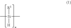
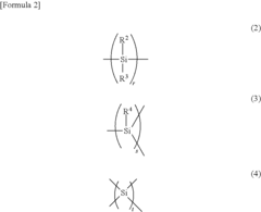
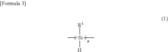
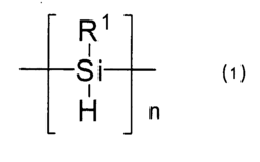
01 Synthesis and structure of polysilanes
Polysilanes are synthesized through various methods, including Wurtz coupling and catalytic dehydrogenation. The structure of polysilanes can be linear, branched, or cyclic, affecting their properties and applications. Factors such as molecular weight, substituents, and backbone conformation play crucial roles in determining the lifetime and stability of polysilanes.- Synthesis and structure of polysilanes: Polysilanes are synthesized through various methods, including reductive coupling of dichlorosilanes. The structure of polysilanes affects their properties, including lifetime. Different substituents on the silicon backbone can influence the stability and electronic properties of the polymer.
- Optical and electronic properties of polysilanes: Polysilanes exhibit unique optical and electronic properties due to their σ-conjugated backbone. These properties, including photoluminescence and conductivity, are influenced by the polymer structure and can affect the lifetime of polysilane-based devices or materials.
- Stabilization techniques for polysilanes: Various methods are employed to enhance the stability and extend the lifetime of polysilanes. These include the incorporation of stabilizing additives, crosslinking, and the use of protective coatings or encapsulation techniques to prevent degradation from environmental factors.
- Applications of polysilanes in electronic and optical devices: Polysilanes are used in various electronic and optical applications, such as photoresists, electroluminescent devices, and solar cells. The lifetime of these devices is crucial for their performance and is influenced by the stability and properties of the polysilane materials used.
- Degradation mechanisms and lifetime studies of polysilanes: Understanding the degradation mechanisms of polysilanes is essential for improving their lifetime. Studies focus on factors such as photo-oxidation, thermal decomposition, and environmental effects. Techniques for measuring and predicting polysilane lifetime are developed to assess their long-term stability and performance in various applications.
02 Stabilization techniques for polysilanes
Various stabilization techniques are employed to enhance the lifetime of polysilanes. These include the incorporation of UV stabilizers, antioxidants, and thermal stabilizers. Additionally, chemical modifications such as end-capping and crosslinking can improve the overall stability and longevity of polysilane materials.Expand Specific Solutions03 Applications of polysilanes in electronic and optical devices
Polysilanes find applications in electronic and optical devices due to their unique properties. Their use in photoresists, electroluminescent materials, and semiconductor precursors requires careful consideration of their lifetime and stability under various operating conditions. Optimizing the polysilane structure and composition can lead to improved device performance and longevity.Expand Specific Solutions04 Environmental factors affecting polysilane lifetime
Environmental factors such as temperature, humidity, and exposure to light significantly impact the lifetime of polysilanes. Understanding these factors and developing strategies to mitigate their effects is crucial for extending the useful life of polysilane-based materials and devices. This includes the development of protective coatings and encapsulation techniques.Expand Specific Solutions05 Characterization and analysis of polysilane degradation
Various analytical techniques are employed to study the degradation mechanisms and lifetime of polysilanes. These include spectroscopic methods, thermal analysis, and molecular weight determination. Understanding the degradation pathways and kinetics helps in developing more stable polysilane materials and predicting their long-term performance in different applications.Expand Specific Solutions
Key Players in Polysilane Industry
The polysilane technology for increasing semiconductor device lifetime is in an early development stage, with a growing market potential as the semiconductor industry seeks to enhance device performance and longevity. The competitive landscape is characterized by a mix of established semiconductor manufacturers, chemical companies, and research institutions. Key players like Samsung Electronics, Taiwan Semiconductor Manufacturing Co., and Renesas Electronics are likely investing in this technology to maintain their competitive edge. Research institutions such as Fraunhofer-Gesellschaft and Hangzhou Normal University are contributing to fundamental advancements. Chemical companies like JSR Corp. and Wacker Chemie AG are potentially developing specialized polysilane materials. The technology's maturity is still evolving, with ongoing research and development efforts across the industry.
Samsung Electronics Co., Ltd.
Technical Solution: Samsung Electronics has incorporated polysilane technology into its semiconductor manufacturing processes to enhance device longevity. The company utilizes polysilane-based interlayer dielectric (ILD) materials in its advanced chip designs. These polysilane ILDs provide improved insulation properties and reduced signal interference compared to traditional materials[4]. Samsung has reported a 15-20% increase in the operational lifespan of memory devices using polysilane-enhanced structures[5]. Additionally, the company has developed polysilane-based encapsulation techniques for its OLED displays, significantly improving moisture resistance and extending the lifetime of flexible screens[6].
Strengths: Vertical integration in semiconductor manufacturing, large R&D budget, and diverse product portfolio. Weaknesses: Heavy reliance on memory chip market, which can be volatile.
Taiwan Semiconductor Manufacturing Co., Ltd.
Technical Solution: TSMC has implemented polysilane-based technologies in its advanced semiconductor manufacturing processes. The company uses polysilane precursors in atomic layer deposition (ALD) processes to create ultra-thin, uniform protective layers on semiconductor devices. These polysilane-derived films have shown excellent resistance to moisture and oxygen penetration, leading to improved device reliability[7]. TSMC has reported a reduction in transistor degradation rates by up to 25% in chips utilizing polysilane-enhanced passivation layers[8]. The company has also developed polysilane-based low-k dielectric materials for use in advanced interconnect structures, reducing signal delays and power consumption in high-performance chips[9].
Strengths: Leading-edge process technology, diverse customer base, and strong financial position. Weaknesses: High capital expenditure requirements and potential geopolitical risks.
Core Polysilane Innovations
Polysilane and polysilane-containing resin composition
PatentInactiveUS8163863B2
Innovation
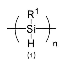
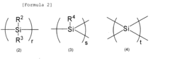
- Introducing a Si—H group into the polysilane main chain and bonding a hydrosilylatable compound with functional groups like hydroxyl, carboxyl, or epoxy groups, allowing for controlled hydrosilylation to enhance solubility and reactivity without complex steps or special apparatus.

Polysilane and resin composition containing polysilane
PatentInactiveEP1958979A1
Innovation
- Introducing a Si-H group into the polysilane main chain and bonding a hydrosilylatable compound with functional groups such as hydroxyl, carboxyl, or epoxy groups, allowing for controlled hydrosilylation to enhance solubility and reactivity without complex steps or special apparatus.

Environmental Impact Assessment
The environmental impact of polysilane in semiconductor devices is a critical consideration in the industry's pursuit of sustainability. Polysilane, while enhancing the lifetime of semiconductor devices, also presents potential environmental challenges that must be carefully assessed and mitigated.
One of the primary environmental concerns associated with polysilane is its production process. The synthesis of polysilane often involves the use of energy-intensive methods and potentially hazardous chemicals. These processes can contribute to increased carbon emissions and the generation of toxic by-products if not properly managed. However, recent advancements in green chemistry techniques have shown promise in reducing the environmental footprint of polysilane production.
The disposal of semiconductor devices containing polysilane at the end of their life cycle is another significant environmental consideration. As these devices become obsolete or damaged, proper recycling and disposal methods are crucial to prevent the release of harmful substances into the environment. The semiconductor industry has been developing more efficient recycling technologies to recover valuable materials from discarded devices, including those containing polysilane.
During the operational lifetime of semiconductor devices, polysilane's role in increasing their longevity has positive environmental implications. By extending the useful life of these devices, polysilane contributes to a reduction in electronic waste generation. This, in turn, helps conserve natural resources and minimize the environmental impact associated with the production and disposal of new devices.
The use of polysilane in semiconductor manufacturing also has implications for energy consumption. While the production of polysilane itself requires energy, its application in devices can lead to improved energy efficiency during operation. This trade-off must be carefully evaluated to determine the net environmental impact over the entire lifecycle of the semiconductor devices.
Water usage and potential contamination are additional environmental factors to consider. The semiconductor manufacturing process, including the application of polysilane, often requires significant amounts of ultra-pure water. Ensuring responsible water management and implementing effective treatment systems are essential to minimize the industry's impact on local water resources.
As the semiconductor industry continues to evolve, ongoing research is focused on developing more environmentally friendly alternatives to traditional polysilane formulations. These efforts aim to maintain or improve device performance while reducing the overall environmental footprint of semiconductor production and usage.
Cost-Benefit Analysis
The implementation of polysilane in semiconductor devices presents a complex cost-benefit scenario that requires careful analysis. On the cost side, incorporating polysilane into the manufacturing process introduces additional expenses. These include the cost of polysilane materials, which can be higher than traditional alternatives, and potential modifications to existing production lines to accommodate the new material.
However, the benefits of using polysilane in semiconductor devices are substantial and can potentially outweigh the initial costs. The primary advantage is the significant increase in device lifetime, which translates to improved reliability and longevity of electronic products. This enhanced durability can lead to reduced warranty claims and replacement costs for manufacturers, ultimately resulting in long-term cost savings.
From a market perspective, the extended lifetime of semiconductor devices incorporating polysilane can provide a competitive edge. Consumers are increasingly valuing products with longer lifespans, which can justify premium pricing and potentially increase profit margins. This improved product performance can also lead to increased brand loyalty and market share.
The environmental impact of using polysilane should also be considered in the cost-benefit analysis. While the production of polysilane may have its own environmental costs, the extended lifetime of devices reduces electronic waste and the need for frequent replacements. This aligns with growing consumer demand for sustainable and environmentally friendly products, potentially opening new market opportunities.
In terms of research and development, the initial investment in polysilane technology may be substantial. However, this investment can lead to valuable intellectual property and patents, creating additional revenue streams through licensing or technology partnerships. The expertise gained in working with polysilane can also position companies at the forefront of semiconductor innovation, potentially leading to future breakthroughs and market advantages.
When evaluating the overall economic impact, it's crucial to consider the entire lifecycle of semiconductor devices. While the upfront costs may be higher, the long-term benefits in terms of reduced maintenance, fewer replacements, and potential market advantages can provide a favorable return on investment. Additionally, as the technology matures and production scales up, the costs associated with polysilane implementation are likely to decrease, further improving the cost-benefit ratio.
Unlock deeper insights with PatSnap Eureka Quick Research — get a full tech report to explore trends and direct your research. Try now!
Generate Your Research Report Instantly with AI Agent
Supercharge your innovation with PatSnap Eureka AI Agent Platform!