How to Evaluate Chiplet Architecture for Mixed-Signal Designs?
JUL 16, 20259 MIN READ
Generate Your Research Report Instantly with AI Agent
Patsnap Eureka helps you evaluate technical feasibility & market potential.
Chiplet Architecture Evolution and Objectives
Chiplet architecture has emerged as a revolutionary approach in the semiconductor industry, offering a paradigm shift in chip design and manufacturing. The evolution of chiplet architecture can be traced back to the early 2010s when the limitations of monolithic chip designs became increasingly apparent. As Moore's Law began to slow down, chiplets presented a viable solution to continue scaling performance and functionality while managing costs and manufacturing complexities.
The primary objective of chiplet architecture is to disaggregate complex system-on-chip (SoC) designs into smaller, more manageable components. This modular approach allows for the integration of diverse technologies and intellectual property (IP) blocks, each optimized for specific functions. In the context of mixed-signal designs, chiplets offer unique advantages by enabling the separation of analog and digital components, which can be fabricated using different process nodes optimized for their respective requirements.
The evolution of chiplet architecture has been driven by several key factors. First, the increasing demand for heterogeneous integration, where different types of chips or IP blocks need to work together seamlessly. Second, the need to overcome the limitations of monolithic designs in terms of yield, cost, and time-to-market. Third, the push for more flexible and scalable chip designs that can be easily customized for different applications and market segments.
As chiplet technology has matured, several key objectives have emerged. One primary goal is to establish standardized interfaces and protocols for chiplet-to-chiplet communication, such as the Advanced Interface Bus (AIB) and Universal Chiplet Interconnect Express (UCIe). These standards aim to create an ecosystem where chiplets from different vendors can be easily integrated, fostering innovation and competition in the semiconductor industry.
Another critical objective is to improve the energy efficiency and performance of mixed-signal designs. By allowing analog and digital components to be fabricated separately and then integrated, chiplet architecture enables each component to be optimized for its specific requirements. This approach can lead to significant improvements in overall system performance and power consumption.
The evaluation of chiplet architecture for mixed-signal designs must consider several key aspects. These include the performance of inter-chiplet communication, the effectiveness of power management across multiple chiplets, the thermal characteristics of the integrated package, and the overall system reliability. Additionally, the evaluation should assess the flexibility and scalability of the chiplet-based design, as well as its potential for future upgrades and modifications.
As chiplet technology continues to evolve, new objectives are emerging. These include the development of advanced packaging technologies to support higher bandwidth and lower latency inter-chiplet communication, as well as the creation of design tools and methodologies specifically tailored for chiplet-based systems. The ultimate goal is to establish chiplet architecture as a mainstream approach for complex mixed-signal designs, enabling the semiconductor industry to continue delivering innovative solutions in the post-Moore's Law era.
Mixed-Signal Design Market Analysis
The mixed-signal design market has experienced significant growth in recent years, driven by the increasing demand for integrated circuits that combine analog and digital functionalities. This market segment is crucial for various applications, including automotive electronics, consumer devices, industrial automation, and telecommunications.
The global mixed-signal IC market was valued at approximately $97.27 billion in 2020 and is projected to reach $149.80 billion by 2026, growing at a CAGR of 7.5% during the forecast period. This growth is primarily attributed to the rising adoption of IoT devices, smart sensors, and the increasing complexity of electronic systems across multiple industries.
In the context of chiplet architecture for mixed-signal designs, the market analysis reveals several key trends and opportunities. The chiplet approach, which involves integrating multiple smaller dies into a single package, is gaining traction in the mixed-signal domain due to its potential to improve performance, reduce costs, and enhance design flexibility.
The automotive sector is emerging as a significant driver for mixed-signal chiplet architectures. Advanced driver assistance systems (ADAS) and autonomous vehicles require sophisticated sensor fusion and signal processing capabilities, which can benefit from the modular nature of chiplet designs. The automotive mixed-signal IC market is expected to grow at a CAGR of 8.2% from 2021 to 2026.
Consumer electronics, particularly smartphones and wearable devices, represent another major market segment for mixed-signal chiplet architectures. These devices demand high-performance, low-power solutions that can integrate various analog and digital functions within a compact form factor. The consumer electronics segment accounted for 35% of the mixed-signal IC market in 2020.
The industrial and healthcare sectors are also showing increased interest in mixed-signal chiplet designs. Industrial IoT applications require robust, high-precision analog front-ends combined with powerful digital processing capabilities. Similarly, medical devices and diagnostic equipment benefit from the integration of sensitive analog sensors with advanced digital signal processing.
Geographically, Asia-Pacific dominates the mixed-signal IC market, accounting for 45% of the global market share in 2020. This region, led by countries like China, South Korea, and Taiwan, is expected to maintain its leadership position due to the presence of major semiconductor manufacturers and the growing electronics industry.
North America and Europe follow as key markets for mixed-signal chiplet architectures, driven by innovation in automotive electronics, aerospace, and defense applications. These regions are home to several leading chiplet technology developers and are expected to contribute significantly to market growth.
Chiplet Challenges in Mixed-Signal Integration
The integration of mixed-signal designs into chiplet architectures presents several significant challenges that must be addressed to ensure optimal performance and functionality. One of the primary obstacles is the management of signal integrity across chiplet interfaces. Mixed-signal designs often require precise timing and low-noise environments, which can be compromised when signals traverse between chiplets. The interconnects between chiplets introduce additional parasitic elements, potentially leading to signal degradation, increased jitter, and reduced overall system performance.
Power distribution and thermal management pose another set of challenges in mixed-signal chiplet integration. Different chiplets may have varying power requirements and thermal characteristics, necessitating sophisticated power delivery networks and cooling solutions. Ensuring stable power supply and minimizing thermal gradients across the chiplet assembly is crucial for maintaining the accuracy of analog components and the reliability of digital circuits.
The heterogeneous nature of mixed-signal designs further complicates chiplet integration. Analog and digital components often require different process technologies, which can lead to incompatibilities when attempting to combine them in a single chiplet or across multiple chiplets. This heterogeneity may result in increased design complexity, longer development cycles, and potential yield issues during manufacturing.
Testing and validation of mixed-signal chiplet designs present unique challenges. Traditional testing methodologies may not be sufficient to verify the performance of integrated analog and digital functions across chiplet boundaries. Developing comprehensive test strategies that can effectively assess both individual chiplet functionality and system-level performance is essential but often requires innovative approaches and specialized equipment.
Packaging and assembly techniques for mixed-signal chiplet designs must also be carefully considered. The choice of packaging materials, interconnect technologies, and assembly processes can significantly impact signal integrity, thermal performance, and overall system reliability. Advanced packaging solutions, such as 2.5D and 3D integration, offer potential benefits but also introduce additional complexities in terms of design, manufacturing, and cost.
Standardization and interoperability remain ongoing challenges in the chiplet ecosystem, particularly for mixed-signal designs. The lack of universally accepted standards for chiplet interfaces and protocols can hinder the development of modular and reusable mixed-signal components. Establishing industry-wide standards that address the specific requirements of mixed-signal integration is crucial for promoting wider adoption of chiplet-based architectures in this domain.
Current Evaluation Methods for Chiplet Architectures
01 Interconnect optimization for chiplet architecture
Improving the performance of chiplet architectures through optimized interconnect designs. This includes advanced packaging technologies, high-bandwidth interfaces, and efficient communication protocols between chiplets to reduce latency and increase data transfer rates.- Interconnect optimization for chiplet performance: Chiplet architectures focus on optimizing interconnects between different chiplets to enhance overall system performance. This includes developing advanced packaging technologies, high-bandwidth interfaces, and efficient communication protocols to minimize latency and maximize data transfer rates between chiplets.
- Power management in chiplet designs: Effective power management strategies are crucial for chiplet architectures to optimize performance while maintaining energy efficiency. This involves implementing dynamic voltage and frequency scaling, power gating, and thermal management techniques across multiple chiplets to balance power consumption and heat dissipation.
- Memory integration and hierarchy in chiplet systems: Chiplet architectures incorporate innovative memory integration techniques to improve system performance. This includes implementing high-bandwidth memory (HBM) stacks, optimizing cache hierarchies across chiplets, and developing efficient memory coherence protocols to enhance data access and processing capabilities.
- Heterogeneous integration of chiplets: Chiplet architectures leverage heterogeneous integration to combine different types of chiplets, such as CPUs, GPUs, AI accelerators, and specialized processors. This approach allows for optimized performance in specific workloads while maintaining flexibility and scalability in system design.
- Thermal management and cooling solutions for chiplet designs: Effective thermal management is critical for maintaining optimal performance in chiplet architectures. This involves developing advanced cooling solutions, such as liquid cooling, microchannel heat sinks, and thermal interface materials, to efficiently dissipate heat from densely packed chiplets and ensure consistent performance under various workloads.
02 Power management in chiplet-based systems
Implementing sophisticated power management techniques for chiplet architectures to enhance overall system efficiency. This involves dynamic voltage and frequency scaling, power gating, and thermal management strategies tailored for multi-chiplet designs.Expand Specific Solutions03 Memory integration and optimization for chiplets
Enhancing chiplet performance through innovative memory integration techniques. This includes high-bandwidth memory (HBM) stacking, cache coherency protocols for distributed memory systems, and optimized memory controllers for chiplet-based architectures.Expand Specific Solutions04 Heterogeneous integration in chiplet designs
Improving chiplet architecture performance by integrating diverse types of chiplets, such as CPUs, GPUs, AI accelerators, and specialized processing units. This approach allows for optimized task-specific processing and improved overall system performance.Expand Specific Solutions05 Thermal management and cooling solutions for chiplet architectures
Developing advanced thermal management and cooling solutions specifically designed for chiplet-based systems. This includes innovative heat spreading techniques, liquid cooling systems, and thermal-aware chiplet placement strategies to maintain optimal performance under various workloads.Expand Specific Solutions
Key Players in Chiplet Ecosystem
The chiplet architecture for mixed-signal designs is in a nascent stage of development, with the market showing significant growth potential. The technology is still evolving, with varying levels of maturity across different companies. Key players like Intel, AMD, and Cadence are at the forefront, leveraging their expertise in semiconductor design and EDA tools. Companies such as Micron and NXP are also making strides in this field, focusing on memory and automotive applications respectively. The competitive landscape is dynamic, with both established semiconductor giants and specialized design firms vying for market share. As the technology matures, we can expect increased collaboration and standardization efforts to drive wider adoption across various industries.
Intel Corp.
Technical Solution: Intel's approach to evaluating chiplet architecture for mixed-signal designs involves their Advanced Interface Bus (AIB) technology. AIB enables high-bandwidth, low-power die-to-die communication, crucial for mixed-signal chiplets[1]. They utilize a modular design methodology, allowing for the integration of analog and digital components on separate chiplets. Intel's evaluation process includes comprehensive signal integrity analysis, thermal modeling, and power distribution simulations[2]. They employ advanced packaging technologies like EMIB (Embedded Multi-die Interconnect Bridge) to optimize interconnects between chiplets[3]. Intel also focuses on standardization efforts, participating in the development of Universal Chiplet Interconnect Express (UCIe) to ensure interoperability and streamline evaluation processes[4].
Strengths: Extensive experience in chiplet design, strong R&D capabilities, and leadership in industry standardization efforts. Weaknesses: Potential complexity in integrating diverse IP blocks and managing thermal challenges in dense chiplet configurations.
Cadence Design Systems, Inc.
Technical Solution: Cadence's approach to evaluating chiplet architecture for mixed-signal designs centers on their Integrity 3D-IC platform. This comprehensive solution enables system planning, implementation, and analysis of multi-chiplet designs[5]. For mixed-signal evaluation, Cadence employs advanced simulation tools that can model both analog and digital components simultaneously, ensuring accurate performance predictions[6]. Their methodology includes detailed power analysis, thermal simulation, and signal integrity verification across chiplet interfaces. Cadence also provides IP for chiplet-based designs, including SerDes and PHY interfaces optimized for die-to-die communication[7]. Their evaluation process incorporates machine learning algorithms to optimize chiplet placement and routing, enhancing overall system performance and reliability[8].
Strengths: Comprehensive design and verification tools, expertise in mixed-signal simulation, and advanced AI-driven optimization. Weaknesses: Potential learning curve for new users and integration challenges with third-party tools.
Innovative Chiplet Interconnect Technologies
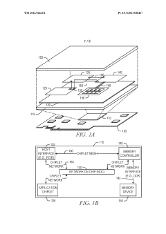
Flow control for a multiple flow control unit interface
PatentWO2022046254A1
Innovation
- Implementing a credit-based flow control system that uses a credit return field to indicate available buffer space, allowing credits to be returned based on transfer cycles rather than individual flits, thereby reducing the number of data packets needed for credit return and minimizing processing overhead.

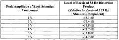
System and method for indentifying a signature of a device, in a communication circuit, utilizing distortion products
PatentWO2006012231A2
Innovation
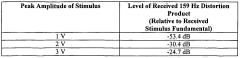
- A system and method utilizing a stimulus signal generator to produce signals at varying amplitudes, exceeding a threshold to elicit signature signals, and an evaluation device to assess intermodulation distortion products, allowing for the identification and classification of communication circuit devices based on the amplitude of these distortion products.

Standardization Efforts in Chiplet Design
Standardization efforts in chiplet design have become increasingly crucial as the industry moves towards more modular and heterogeneous integrated circuit architectures. These efforts aim to establish common interfaces, protocols, and design methodologies that enable seamless integration of diverse chiplets from different vendors.
One of the primary standardization initiatives is the Universal Chiplet Interconnect Express (UCIe), which focuses on defining a die-to-die interconnect standard for chiplets. UCIe aims to create an open ecosystem that allows for the mixing and matching of chiplets from various manufacturers, promoting interoperability and reducing design complexity.
Another significant standardization effort is the Advanced Interface Bus (AIB), developed by Intel. AIB provides a standardized interface for high-bandwidth, low-latency communication between chiplets. This standard has gained traction in the industry and is being adopted by several manufacturers for their chiplet designs.
The Open Compute Project (OCP) has also contributed to chiplet standardization through its Open Domain-Specific Architecture (ODSA) workgroup. ODSA focuses on developing open architectures and standards for chiplet-based designs, including the Bunch of Wires (BoW) interface specification.
In the realm of mixed-signal designs, standardization efforts are addressing the unique challenges posed by integrating analog and digital components. The CHIPS Alliance, a consortium of companies and organizations, is working on developing open-source tools and methodologies for chiplet-based designs, including those with mixed-signal elements.
Standardization bodies such as JEDEC and IEEE are also actively involved in developing standards related to chiplet architectures. These efforts encompass various aspects, including thermal management, power delivery, and testing methodologies for chiplet-based systems.
As the chiplet ecosystem continues to evolve, standardization efforts are expanding to address emerging challenges. These include the development of standards for 2.5D and 3D integration technologies, which are becoming increasingly important for high-performance mixed-signal designs.
The success of these standardization efforts will be crucial in realizing the full potential of chiplet architectures for mixed-signal designs. By establishing common frameworks and interfaces, these initiatives aim to reduce design complexity, improve interoperability, and accelerate time-to-market for chiplet-based products.
Thermal Management in Mixed-Signal Chiplets
Thermal management is a critical aspect of mixed-signal chiplet design, as it directly impacts performance, reliability, and power efficiency. In mixed-signal chiplets, the coexistence of analog and digital components presents unique challenges for heat dissipation and temperature control. The thermal characteristics of analog circuits are particularly sensitive, as temperature variations can significantly affect their performance and accuracy.
To address these challenges, several thermal management strategies have been developed for mixed-signal chiplets. One approach involves the strategic placement of analog and digital components within the chiplet to optimize heat distribution. By carefully arranging heat-generating elements and incorporating thermal barriers, designers can minimize thermal coupling between sensitive analog circuits and high-power digital blocks.
Advanced packaging technologies play a crucial role in thermal management for mixed-signal chiplets. Three-dimensional integrated circuits (3D-ICs) and through-silicon vias (TSVs) enable vertical stacking of chiplets, which can improve thermal performance by reducing the overall footprint and allowing for more efficient heat dissipation. Additionally, the use of advanced thermal interface materials (TIMs) between chiplets and heat spreaders enhances thermal conductivity and reduces thermal resistance.
Active cooling techniques are also employed in mixed-signal chiplet designs. Microfluidic cooling channels integrated within the chiplet or package can provide localized cooling to critical areas. These channels allow for the circulation of coolants, effectively removing heat from high-power regions and maintaining optimal operating temperatures for sensitive analog components.
Thermal sensors and dynamic thermal management systems are increasingly being incorporated into mixed-signal chiplets. These sensors monitor temperature variations across the chiplet in real-time, allowing for adaptive power management and thermal control. By dynamically adjusting clock frequencies, voltage levels, and power states of individual components, the overall thermal profile of the chiplet can be optimized to maintain performance while preventing thermal runaway.
Simulation and modeling tools play a vital role in the thermal management of mixed-signal chiplets. Advanced thermal modeling techniques, such as computational fluid dynamics (CFD) and finite element analysis (FEA), enable designers to predict and analyze thermal behavior during the design phase. These tools help identify potential hotspots, optimize component placement, and evaluate the effectiveness of various cooling strategies before physical prototyping.
Unlock deeper insights with Patsnap Eureka Quick Research — get a full tech report to explore trends and direct your research. Try now!
Generate Your Research Report Instantly with AI Agent
Supercharge your innovation with Patsnap Eureka AI Agent Platform!