Impact of 2D Semiconductors on Aerospace Standards
OCT 14, 202510 MIN READ
Generate Your Research Report Instantly with AI Agent
Patsnap Eureka helps you evaluate technical feasibility & market potential.
2D Semiconductor Evolution and Aerospace Integration Goals
Two-dimensional (2D) semiconductors represent a revolutionary class of materials that have emerged from the broader family of 2D materials, first popularized by graphene's discovery in 2004. Unlike traditional bulk semiconductors, these atomically thin materials exhibit unique quantum confinement effects that dramatically alter their electronic, optical, and mechanical properties. The evolution of 2D semiconductors has progressed rapidly over the past decade, moving from laboratory curiosities to materials with genuine technological potential, particularly in aerospace applications where weight, power efficiency, and reliability under extreme conditions are paramount concerns.
The historical trajectory of 2D semiconductor development began with transition metal dichalcogenides (TMDs) such as MoS2 and WS2, which demonstrated semiconductor properties with tunable bandgaps. This was followed by the exploration of other 2D material families including black phosphorus, hexagonal boron nitride (h-BN), and various Xenes (silicene, germanene, stanene). Each evolutionary step has expanded the available property space, enabling more sophisticated aerospace applications.
Current research trends indicate a shift toward heterostructures—artificially stacked layers of different 2D materials—which create "designer" electronic properties through interlayer interactions. This approach mimics traditional semiconductor heterojunctions but with atomic precision and novel quantum effects that could revolutionize aerospace electronics.
For aerospace integration, the primary goals center on leveraging the unique advantages of 2D semiconductors to enhance performance metrics critical to flight systems. These include developing radiation-hardened electronics that maintain functionality in the harsh space environment, creating ultra-lightweight sensor arrays for structural health monitoring, and designing high-efficiency power management systems that reduce overall spacecraft weight and power consumption.
The integration roadmap encompasses near-term goals of incorporating 2D materials into existing aerospace systems as performance enhancers, mid-term objectives of developing hybrid systems that combine traditional and 2D semiconductor technologies, and long-term visions of all-2D electronic systems that fundamentally reimagine aerospace capabilities.
Technical challenges that must be addressed include scalable manufacturing processes compatible with aerospace quality standards, reliable encapsulation methods to protect 2D materials from environmental degradation, and standardized testing protocols to validate performance under aerospace conditions. These challenges form the foundation of current research initiatives across both academic and industrial sectors focused on aerospace applications.
Aerospace Market Demand for Advanced Semiconductor Solutions
The aerospace industry is experiencing a significant shift towards more advanced electronic systems that require superior semiconductor solutions. Current market analysis indicates a growing demand for lightweight, radiation-resistant, and high-performance semiconductor components that can withstand the extreme conditions of space and high-altitude operations. This demand is primarily driven by the expansion of satellite constellations, increased space exploration missions, and the modernization of aircraft systems.
The global aerospace semiconductor market has been steadily growing, with particular emphasis on solutions that offer reduced size, weight, and power consumption (SWaP). Traditional silicon-based semiconductors are reaching their physical limitations in meeting these requirements, creating a substantial market opportunity for next-generation semiconductor technologies, particularly 2D semiconductors like graphene, molybdenum disulfide, and hexagonal boron nitride.
Commercial satellite operators are increasingly seeking advanced semiconductor solutions to enhance communication capabilities, improve data processing, and extend operational lifespans. The proliferation of small satellite constellations for Earth observation, communication, and scientific research has created a demand surge for specialized semiconductor components that can operate reliably in the harsh space environment while consuming minimal power.
Defense and military aerospace applications represent another significant market segment, with requirements for secure, radiation-hardened semiconductor solutions that can maintain functionality under extreme conditions. These applications demand semiconductors with enhanced resistance to single-event effects (SEEs) and total ionizing dose (TID) radiation, areas where 2D semiconductors show promising characteristics.
Aircraft manufacturers are also driving demand for advanced semiconductor solutions as they move toward more electric aircraft (MEA) designs. These designs require power electronics capable of handling higher voltages and temperatures while maintaining efficiency and reliability. The integration of more sophisticated avionics systems, autonomous flight capabilities, and enhanced connectivity features further increases the need for high-performance semiconductor components.
The unmanned aerial vehicle (UAV) sector presents additional market opportunities, with requirements for lightweight, energy-efficient semiconductors that can support extended flight times and enhanced sensing capabilities. As UAVs become more prevalent in both commercial and military applications, the demand for specialized semiconductor solutions continues to grow.
Market forecasts indicate that aerospace-grade semiconductor solutions will need to address several key performance parameters: radiation hardness, thermal management, power efficiency, reliability at extreme temperatures, and long-term stability. 2D semiconductors show particular promise in addressing these requirements due to their unique physical and electronic properties, positioning them as potentially transformative technologies for next-generation aerospace systems.
Current State and Challenges of 2D Semiconductors in Aerospace
The integration of 2D semiconductors into aerospace applications represents a significant technological frontier with both promising advancements and substantial challenges. Currently, 2D semiconductor materials such as graphene, molybdenum disulfide (MoS2), and hexagonal boron nitride (h-BN) are transitioning from laboratory research to practical aerospace implementations, albeit at varying stages of technological readiness.
In the aerospace sector, 2D semiconductors have demonstrated exceptional properties including high electron mobility, mechanical flexibility, thermal stability, and radiation hardness. These characteristics make them particularly attractive for space-based electronics that must withstand extreme environmental conditions. Several aerospace entities, including NASA, ESA, and major defense contractors, have initiated research programs focused on 2D semiconductor integration into satellite systems, avionics, and sensor networks.
Despite these promising developments, significant technical challenges persist. Manufacturing scalability remains a primary obstacle, with current production methods unable to consistently produce large-area, defect-free 2D semiconductor films at volumes necessary for aerospace applications. The aerospace industry's stringent reliability requirements demand semiconductor materials with defect densities orders of magnitude lower than currently achievable.
Integration challenges also present substantial hurdles. Interfacing 2D materials with conventional electronics requires novel bonding techniques and interface engineering to maintain performance advantages. Additionally, encapsulation technologies must be developed to protect these atomically thin materials from environmental degradation in space conditions, including atomic oxygen exposure and radiation damage.
Standardization represents another critical challenge. The aerospace industry operates under rigorous certification frameworks such as DO-254 for hardware and MIL-STD-883 for microelectronics. Currently, no standardized testing protocols exist specifically for 2D semiconductor components in aerospace applications, creating uncertainty in qualification processes and hindering widespread adoption.
Geographically, research leadership in 2D aerospace semiconductors shows distinct patterns. The United States maintains strong positions through NASA, DARPA, and university research clusters. The European Union has established dedicated programs through Horizon Europe and ESA initiatives. China has rapidly accelerated investments in both fundamental research and applications development, while South Korea and Japan focus on specialized applications leveraging their semiconductor manufacturing expertise.
Funding constraints further complicate advancement, as the extended qualification timeline for aerospace components (often 5-10 years) exceeds typical investment horizons. This creates a "valley of death" where promising technologies struggle to transition from laboratory demonstrations to flight-qualified hardware, necessitating sustained government and industry consortium support.
Current Implementation Solutions for Aerospace Applications
01 2D Semiconductor Materials and Fabrication
Two-dimensional semiconductor materials represent a class of materials with unique electronic properties due to their atomic-scale thickness. These materials, including transition metal dichalcogenides, graphene derivatives, and other layered compounds, exhibit exceptional electrical, optical, and mechanical characteristics. Fabrication techniques for these materials include mechanical exfoliation, chemical vapor deposition, and molecular beam epitaxy, which allow for precise control over layer thickness and composition.- Materials and fabrication of 2D semiconductors: Two-dimensional semiconductor materials, such as transition metal dichalcogenides, graphene derivatives, and other atomically thin materials, are being developed for next-generation electronic applications. These materials exhibit unique electronic properties when reduced to single or few-layer thickness. Various fabrication methods including chemical vapor deposition, mechanical exfoliation, and epitaxial growth are employed to create these ultra-thin semiconductor layers with precise control over thickness and composition.
- Electronic devices based on 2D semiconductors: Two-dimensional semiconductors are being integrated into various electronic devices including transistors, memory cells, sensors, and logic circuits. These materials enable the development of ultra-thin, flexible electronic components with improved performance characteristics such as higher carrier mobility, better electrostatic control, and reduced power consumption. The atomically thin nature of these semiconductors allows for more efficient scaling of electronic devices beyond traditional silicon technology limitations.
- Optoelectronic applications of 2D semiconductors: Two-dimensional semiconductors exhibit unique optical properties that make them suitable for various optoelectronic applications. These materials feature direct bandgaps that can be tuned through thickness control, strain engineering, or heterostructure formation. Applications include photodetectors, light-emitting diodes, photovoltaic cells, and optical modulators. The strong light-matter interaction in atomically thin layers enables highly efficient optoelectronic devices with reduced material consumption.
- Heterostructures and interfaces in 2D semiconductor systems: Vertical stacking of different 2D materials creates heterostructures with novel electronic and optical properties not found in individual layers. These van der Waals heterostructures enable band alignment engineering, interlayer excitons, and quantum confinement effects. Interface engineering between 2D semiconductors and other materials (including substrates, dielectrics, and metals) is crucial for optimizing device performance and enabling new functionalities in areas such as quantum computing and spintronics.
- Computational modeling and characterization of 2D semiconductors: Advanced computational methods and characterization techniques are essential for understanding and predicting the properties of 2D semiconductor materials. These include density functional theory calculations, molecular dynamics simulations, and machine learning approaches for material discovery and property prediction. Various analytical techniques such as scanning probe microscopy, transmission electron microscopy, and spectroscopic methods are employed to characterize the structural, electronic, and optical properties of these atomically thin materials.
02 Electronic Devices Based on 2D Semiconductors
2D semiconductors enable the development of ultra-thin electronic devices with enhanced performance characteristics. These materials are incorporated into field-effect transistors, memory devices, sensors, and integrated circuits that benefit from their unique electronic band structures and carrier transport properties. The atomically thin nature of these materials allows for excellent electrostatic control, reduced short-channel effects, and potential for flexible electronics applications.Expand Specific Solutions03 Optoelectronic Applications of 2D Semiconductors
2D semiconductor materials exhibit distinctive optical properties that make them suitable for various optoelectronic applications. Their direct bandgaps, strong light-matter interactions, and tunable optical responses enable the development of photodetectors, light-emitting diodes, photovoltaic cells, and optical modulators. These materials demonstrate high absorption coefficients, photoluminescence, and valley-selective optical excitation that can be leveraged for next-generation optoelectronic devices.Expand Specific Solutions04 Heterostructures and Interface Engineering
Vertical stacking of different 2D materials creates heterostructures with tailored electronic and optical properties. These van der Waals heterostructures exhibit unique interlayer interactions that can be engineered to achieve specific functionalities. Interface engineering techniques, including controlled doping, defect management, and contact optimization, are crucial for enhancing device performance. The atomically sharp interfaces between layers enable novel quantum phenomena and device architectures not possible with conventional semiconductor technologies.Expand Specific Solutions05 Integration and Manufacturing Technologies
Integrating 2D semiconductors into conventional semiconductor manufacturing processes presents both challenges and opportunities. Techniques for large-scale production, transfer methods, and compatibility with existing fabrication infrastructure are critical for commercial viability. Advanced manufacturing approaches include roll-to-roll processing, selective area growth, and automated transfer systems that maintain material quality while enabling industrial-scale production. These integration technologies address issues related to contamination, defects, and process variability that can affect device performance and reliability.Expand Specific Solutions
Key Industry Players in Aerospace 2D Semiconductor Development
The 2D semiconductor market in aerospace is in an early growth phase, characterized by significant R&D investment but limited commercial deployment. Market size remains modest but is projected to expand rapidly as these materials offer advantages in weight reduction, power efficiency, and thermal management critical for aerospace applications. Technologically, the field shows varying maturity levels across players: established semiconductor giants like TSMC, Samsung, and Intel are leveraging their manufacturing expertise to develop aerospace-grade 2D materials; aerospace specialists like Raytheon and Safran are focusing on integration and certification; while academic institutions (MIT, Tsinghua, Peking University) lead fundamental research. The collaboration between industry and academia is accelerating standardization efforts, though widespread adoption awaits further reliability testing and aerospace certification compliance.
Taiwan Semiconductor Manufacturing Co., Ltd.
Technical Solution: TSMC has developed specialized fabrication processes for 2D semiconductor materials targeting aerospace applications, with particular focus on maintaining atomic-level precision at scale. Their approach centers on integrating graphene, hexagonal boron nitride (h-BN), and transition metal dichalcogenides (TMDs) into existing semiconductor manufacturing flows while ensuring compliance with aerospace quality standards. TSMC's technology enables the production of ultra-thin, flexible electronic components that can withstand the extreme temperature variations, radiation exposure, and mechanical stress encountered in aerospace environments. The company has pioneered methods for creating reliable electrical contacts to 2D materials—a critical challenge for aerospace applications—achieving contact resistance values below 200 Ω·μm while maintaining stability through thermal cycling tests designed to simulate aerospace conditions. Their manufacturing processes incorporate specialized contamination control protocols that exceed typical semiconductor standards to address the unique sensitivity of 2D materials, enabling production yields suitable for aerospace qualification requirements.
Strengths: World-leading semiconductor manufacturing infrastructure; established quality control systems adaptable to aerospace standards; advanced process development capabilities. Weaknesses: Limited direct aerospace industry experience; primarily focused on manufacturing rather than system design; need for partnerships with aerospace certification specialists.
Intel Corp.
Technical Solution: Intel has developed a comprehensive 2D semiconductor platform targeting aerospace computing applications, with particular emphasis on low-power, radiation-tolerant processing units. Their approach leverages transition metal dichalcogenide (TMD) materials integrated with conventional silicon architecture to create hybrid computing solutions that meet stringent aerospace reliability standards while delivering enhanced performance. Intel's 2D semiconductor technology incorporates specialized fabrication techniques that ensure uniform material quality across large wafers, addressing a key challenge in scaling 2D materials for aerospace applications. The company has demonstrated functional prototypes of memory and logic devices using 2D materials that maintain operational stability under simulated space radiation conditions, showing performance degradation of less than 5% after exposure equivalent to 5 years in low Earth orbit. Intel's roadmap includes progressive integration of 2D semiconductors into aerospace-grade processors, with initial focus on non-critical systems to establish reliability data before expanding to mission-critical applications.
Strengths: Extensive semiconductor manufacturing expertise; established quality control systems adaptable to aerospace standards; strong position in high-reliability computing markets. Weaknesses: Limited specific aerospace certification experience; primarily focused on computing rather than comprehensive aerospace systems; longer timeline to full 2D semiconductor implementation compared to hybrid approaches.
Critical Patents and Research in 2D Semiconductor Technology
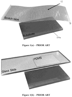
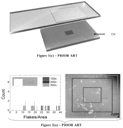
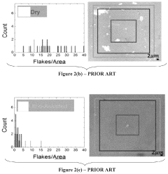
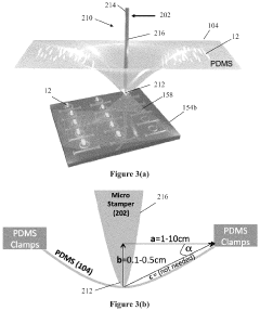
Two-dimensional material printer and transfer system and method for atomically layered materials
PatentActiveUS11999146B2
Innovation
- A micro-stamper-based 2D printer system uses a PDMS gel to precisely transfer 2D materials onto substrates, minimizing cross-contamination by aligning and transferring only the desired flake with high accuracy, eliminating the need for PMMA coatings and reducing mechanical stress on sensitive devices.
Methods and systems for ultra-high quality gated hybrid devices and sensors
PatentActiveUS20160172479A1
Innovation
- A method involving a first substrate with metallization and a second substrate with semiconductor structures, where the two are brought into physical contact without processing the 2DEG wafer, allowing for the use of lower-cost silicon substrates and enabling the reuse and testing of different 2DEG materials on the same device design.
Aerospace Certification and Compliance Requirements
The aerospace industry operates under stringent regulatory frameworks that ensure safety, reliability, and performance of all components used in aircraft and spacecraft systems. The emergence of 2D semiconductors presents both opportunities and challenges for aerospace certification processes. These novel materials must meet or exceed existing standards while potentially necessitating updates to certification protocols to accommodate their unique properties.
Current aerospace certification standards such as DO-254 for hardware and DO-178C for software were developed primarily with traditional semiconductor technologies in mind. The introduction of 2D semiconductor materials like graphene, molybdenum disulfide, and hexagonal boron nitride requires careful evaluation against these established requirements. Particularly, the radiation hardness specifications outlined in MIL-STD-883 Method 1019 must be thoroughly assessed, as 2D materials exhibit different responses to radiation environments encountered in aerospace applications.
The Federal Aviation Administration (FAA) and European Union Aviation Safety Agency (EASA) maintain strict compliance requirements for electronic components, with emphasis on reliability testing under extreme conditions. 2D semiconductors must demonstrate compliance with temperature cycling (−55°C to +125°C), vibration resistance, and humidity testing protocols. Their novel physical properties may necessitate modified test procedures to accurately assess performance boundaries.
Qualification testing for 2D semiconductor components presents unique challenges due to their atomically thin structure. Traditional reliability assessment methods such as accelerated life testing may require adaptation to properly evaluate failure mechanisms specific to these materials. The aerospace industry typically requires components to demonstrate mean time between failures (MTBF) exceeding 100,000 hours, a benchmark that 2D semiconductor devices must achieve through rigorous validation.
Supply chain considerations also impact certification processes, as aerospace standards require traceability and consistency in manufacturing. The relatively nascent production methods for 2D semiconductors must evolve to meet AS9100 quality management requirements and establish repeatable fabrication processes that satisfy aerospace documentation and change control protocols.
International standardization bodies including RTCA, SAE, and JEDEC are beginning to address the integration of 2D semiconductor technologies into existing frameworks. Working groups are developing supplementary guidance for qualification and certification of these advanced materials, with particular focus on their unique electrical, thermal, and mechanical characteristics that fall outside traditional semiconductor parameters.
Space Radiation Effects on 2D Semiconductor Performance
Space radiation presents a significant challenge for semiconductor devices in aerospace applications, with 2D semiconductors exhibiting unique responses compared to traditional silicon-based technologies. When exposed to the harsh radiation environment of space, 2D materials such as graphene, molybdenum disulfide (MoS2), and hexagonal boron nitride (h-BN) demonstrate distinctive degradation mechanisms and performance alterations.
The primary radiation effects on 2D semiconductors include displacement damage, ionization effects, and single event phenomena. Displacement damage occurs when high-energy particles displace atoms from their lattice positions, creating vacancies and interstitials that serve as scattering centers and trap sites. This damage mechanism particularly affects carrier mobility and concentration in 2D materials, though at different rates than in bulk semiconductors.
Ionization effects in 2D semiconductors manifest through charge trapping at interfaces and within supporting substrates. The atomically thin nature of these materials creates a unique situation where radiation-induced charges in adjacent layers significantly influence device performance. Studies have shown that graphene-based devices often exhibit increased conductivity post-irradiation due to doping effects from substrate-trapped charges, while transition metal dichalcogenides (TMDs) typically show threshold voltage shifts and mobility degradation.
Single event effects (SEEs) in 2D semiconductor devices present a complex picture. The reduced volume of active material theoretically lowers the cross-section for particle strikes, potentially reducing susceptibility to single event upsets. However, the lower energy required to disrupt the crystalline structure of atomically thin materials can counteract this advantage in certain radiation environments.
Experimental data from radiation testing of 2D semiconductor devices reveals interesting resilience characteristics. Graphene-based field-effect transistors have demonstrated remarkable radiation hardness against total ionizing dose effects, with some studies reporting functional devices after exposure to doses exceeding 1 Mrad(Si). MoS2 transistors show more complex behavior, with performance degradation occurring primarily through interface and substrate effects rather than direct material damage.
Temperature plays a critical role in radiation response, with cryogenic and elevated temperatures modifying damage mechanisms in 2D materials. At low temperatures, reduced thermal energy limits self-healing processes, while high temperatures can accelerate both damage and recovery processes. This temperature dependence creates additional design considerations for aerospace applications where thermal cycling is common.
The anisotropic nature of 2D materials also influences radiation response, with in-plane and out-of-plane damage mechanisms differing significantly. This directional dependence offers potential design strategies for radiation-hardened 2D semiconductor devices through careful orientation and stacking configurations.
Unlock deeper insights with Patsnap Eureka Quick Research — get a full tech report to explore trends and direct your research. Try now!
Generate Your Research Report Instantly with AI Agent
Supercharge your innovation with Patsnap Eureka AI Agent Platform!