

Lessons From Interop Plugfest For UCIe Chiplet Interconnect
SEP 1, 20259 MIN READ
Generate Your Research Report Instantly with AI Agent
PatSnap Eureka helps you evaluate technical feasibility & market potential.
UCIe Chiplet Interconnect Background and Objectives
Universal Chiplet Interconnect Express (UCIe) represents a significant evolution in semiconductor integration technology, emerging as a response to the slowing of Moore's Law and the increasing challenges in traditional monolithic chip scaling. Developed through industry collaboration, UCIe aims to establish an open, standardized die-to-die interconnect that enables heterogeneous integration of chiplets from different vendors within a single package.
The historical context of UCIe traces back to the growing recognition that traditional monolithic chip designs were facing physical and economic limitations. As transistor scaling became more difficult and expensive, the industry began exploring alternative approaches to continue performance improvements. Chiplet-based design emerged as a promising solution, allowing complex systems to be built from smaller, specialized silicon pieces.
UCIe's development represents a convergence of multiple industry efforts to standardize chiplet interfaces. Prior to UCIe, several proprietary and semi-proprietary interconnect technologies existed, including Intel's AIB (Advanced Interface Bus), AMD's Infinity Fabric, and TSMC's LIPINCON. The formation of the UCIe consortium in 2022 marked a significant milestone in unifying these approaches under a common standard.
The primary technical objectives of UCIe include establishing a standardized physical layer, protocol stack, and software interface for die-to-die communication. This standardization aims to enable a robust chiplet ecosystem where components from different manufacturers can interoperate seamlessly. UCIe specifically targets high-bandwidth, low-latency, and energy-efficient communication between chiplets within a package.
From a market perspective, UCIe addresses several critical industry needs. It promises to reduce development costs by enabling reuse of silicon IP across multiple products. It also offers a path to improved yield management by allowing manufacturers to produce smaller dies with higher yield rates and then integrate them into complex systems. Additionally, UCIe supports more flexible product differentiation by enabling mix-and-match approaches to system design.
The technology evolution trend represented by UCIe points toward increasingly disaggregated chip architectures, where specialized functions are implemented in optimized chiplets rather than integrated into monolithic designs. This approach allows each component to be manufactured using the most appropriate process technology for its specific requirements, potentially optimizing both performance and cost.
Recent interoperability plugfests for UCIe have highlighted both the progress made toward these objectives and the remaining challenges in achieving true multi-vendor chiplet integration. These events serve as critical checkpoints in the technology's maturation process, validating the standard's effectiveness while identifying areas requiring further refinement.
Market Demand Analysis for Chiplet-Based Solutions
The chiplet-based design approach is experiencing unprecedented market demand as traditional monolithic chip scaling faces increasing technical and economic challenges. According to recent industry analyses, the global chiplet market is projected to grow at a CAGR of 40% from 2023 to 2028, reaching approximately $25 billion by 2028. This explosive growth is driven by the semiconductor industry's need to overcome the limitations of Moore's Law while maintaining performance improvements and cost efficiency.
The Universal Chiplet Interconnect Express (UCIe) standard has emerged as a critical enabler for this market, with the recent Interop Plugfest demonstrating significant progress in establishing interoperability between chiplets from different vendors. This interoperability is crucial for market adoption, as it allows system integrators to mix and match components from various suppliers, reducing vendor lock-in and fostering innovation.
Primary market demand for chiplet-based solutions comes from high-performance computing sectors, including data centers, AI accelerators, and cloud service providers. These segments require ever-increasing computational power while managing thermal constraints and energy consumption. The chiplet approach allows for heterogeneous integration of specialized processing units, memory, and I/O components, each manufactured using optimal process nodes.
Enterprise customers are particularly interested in chiplet solutions that can deliver performance improvements without proportional increases in power consumption. The disaggregated nature of chiplet designs enables more efficient cooling solutions and better power management, addressing key concerns in data center operations where energy costs represent a significant portion of operational expenses.
Consumer electronics manufacturers are also showing growing interest in chiplet technology, particularly for mobile devices and edge computing applications. The ability to integrate specialized accelerators for AI, graphics, and signal processing alongside general-purpose processors offers significant advantages in performance per watt, a critical metric for battery-powered devices.
Market research indicates that telecommunications equipment manufacturers are evaluating chiplet-based solutions for next-generation networking infrastructure, particularly for 5G and future 6G deployments. The flexibility to upgrade specific components without redesigning entire systems presents compelling total cost of ownership benefits.
The lessons from the UCIe Interop Plugfest highlight the market's readiness for standardized chiplet interfaces. Industry surveys show that 78% of semiconductor companies are actively developing chiplet-based products, with 65% citing standardized interconnects as a critical factor in their decision-making process. This demonstrates the strong market pull for interoperable solutions that can reduce development costs and accelerate time-to-market.
Current State and Challenges in Chiplet Interconnect Technology
The chiplet interconnect technology landscape is currently experiencing rapid evolution, with Universal Chiplet Interconnect Express (UCIe) emerging as a promising standard. The recent UCIe Interop Plugfest demonstrated significant progress in establishing interoperability between chiplets from different vendors, a critical milestone for the industry. Current implementations have achieved data rates of 16-32 GT/s with power efficiency ranging from 0.5-1 pJ/bit, representing substantial improvements over previous interconnect technologies.
Despite these advancements, several technical challenges persist in the chiplet interconnect domain. Signal integrity issues remain prominent, particularly as data rates increase beyond 32 GT/s, where channel loss, crosstalk, and reflections become more pronounced. The industry is still grappling with thermal management challenges, as the dense integration of chiplets creates localized hotspots that can affect performance and reliability. Power delivery across chiplet boundaries continues to be a significant hurdle, with current solutions struggling to maintain consistent voltage levels across high-performance chiplets.
Testing and validation methodologies for chiplet-based systems present another major challenge. The UCIe Plugfest revealed inconsistencies in test procedures and measurement standards across different vendors, highlighting the need for standardized validation protocols. Additionally, the industry faces a knowledge gap in design-for-test strategies specifically tailored for chiplet architectures.
Manufacturing and assembly processes for chiplet integration remain complex and costly. Current micro-bump technologies achieve pitches of approximately 40-55μm, but next-generation applications will require even finer pitches of 20-30μm, pushing the boundaries of existing manufacturing capabilities. Yield management becomes increasingly critical as systems incorporate multiple chiplets, with defects in any single component potentially compromising the entire package.
The ecosystem fragmentation presents a significant obstacle to widespread adoption. While UCIe represents a promising standardization effort, competing standards and proprietary solutions continue to exist, creating market uncertainty. The Plugfest demonstrated that while basic interoperability is achievable, advanced features and optimizations often remain vendor-specific, limiting the full potential of the chiplet approach.
Security considerations have also emerged as a critical challenge, particularly regarding the protection of intellectual property when integrating chiplets from multiple vendors. The industry has yet to establish robust security protocols for authenticating chiplets and securing data transmission between them, an essential requirement for sensitive applications in sectors like finance, healthcare, and defense.
Interop Plugfest Implementation Approaches
01 UCIe architecture and implementation
The Universal Chiplet Interconnect Express (UCIe) architecture provides a standardized approach for chiplet-to-chiplet communication in multi-die systems. This architecture defines protocols, physical interfaces, and electrical specifications that enable interoperability between chiplets from different vendors. The implementation includes die-to-die interfaces, packaging technologies, and interconnect designs that support high-bandwidth, low-latency communication while maintaining signal integrity across chiplet boundaries.- UCIe architecture and protocol specifications: The Universal Chiplet Interconnect Express (UCIe) architecture defines standardized protocols and interfaces for chiplet-to-chiplet communication. It includes specifications for physical layer, protocol layer, and software stack to ensure interoperability between chiplets from different manufacturers. The architecture supports various data rates, link widths, and communication modes to accommodate different performance requirements while maintaining compatibility across implementations.
- Packaging technologies for chiplet integration: Advanced packaging technologies are essential for implementing UCIe-based chiplet designs. These include various approaches such as silicon interposers, organic substrates, and embedded bridge technologies that facilitate high-density interconnections between chiplets. The packaging solutions address thermal management, signal integrity, and power delivery challenges while enabling the high-bandwidth, low-latency connections required for chiplet interoperability in multi-die systems.
- Testing and validation methodologies for UCIe compliance: Ensuring UCIe compliance requires comprehensive testing and validation methodologies. These include specialized test fixtures, automated test equipment, and validation protocols designed to verify electrical characteristics, timing parameters, and protocol adherence. The testing approaches cover both pre-silicon verification through simulation and post-silicon validation using physical test chips to ensure interoperability between chiplets from different vendors.
- Power management and thermal solutions for UCIe implementations: Effective power management and thermal solutions are critical for UCIe chiplet designs. These include dynamic power scaling, thermal sensing and management techniques, and advanced cooling solutions tailored for multi-die packages. The approaches enable efficient operation of heterogeneous chiplets with different power profiles while maintaining signal integrity across the high-speed UCIe interfaces and ensuring reliable operation under various workload conditions.
- Security and authentication mechanisms for chiplet ecosystems: Security and authentication mechanisms are essential for protecting UCIe-based chiplet ecosystems. These include secure boot processes, cryptographic authentication of chiplets, hardware root of trust implementations, and secure key management. The security features ensure that only authorized chiplets can be integrated into a system, protecting against counterfeiting, tampering, and other security threats while maintaining the interoperability benefits of the UCIe standard.
02 Testing and validation methods for UCIe compliance
Various testing and validation methodologies are employed to ensure chiplets comply with UCIe specifications and maintain interoperability. These methods include protocol compliance testing, electrical characterization, signal integrity analysis, and interoperability testing between chiplets from different manufacturers. Test fixtures, specialized equipment, and automated test procedures are used to verify that chiplets meet the required specifications for reliable operation in multi-die systems.Expand Specific Solutions03 Power management and thermal solutions for UCIe implementations
Power management and thermal solutions are critical aspects of UCIe chiplet implementations. These include techniques for dynamic power allocation between chiplets, thermal management across die interfaces, and energy-efficient communication protocols. Advanced cooling solutions, power delivery networks, and thermal interface materials are designed specifically for multi-chiplet packages to ensure reliable operation under various workloads while maintaining the performance benefits of chiplet architectures.Expand Specific Solutions04 UCIe packaging technologies and integration methods
Specialized packaging technologies and integration methods enable effective implementation of UCIe-compliant chiplet systems. These include advanced substrate designs, through-silicon vias (TSVs), microbumps, and other interconnect technologies that facilitate high-density connections between chiplets. Various assembly techniques, such as fan-out wafer-level packaging and silicon interposers, are employed to optimize signal routing, minimize latency, and enhance the overall performance of multi-chiplet systems while ensuring compliance with UCIe standards.Expand Specific Solutions05 Security and authentication mechanisms for UCIe chiplets
Security and authentication mechanisms are integrated into UCIe implementations to ensure trusted communication between chiplets from different vendors. These include secure boot processes, cryptographic authentication protocols, and hardware-based security features that prevent unauthorized access or tampering. Secure key management, trusted execution environments, and hardware root of trust implementations are designed specifically for multi-chiplet architectures to maintain data integrity and confidentiality across chiplet boundaries while preserving interoperability.Expand Specific Solutions
Key Industry Players in Chiplet Ecosystem
The UCIe chiplet interconnect technology is currently in an early growth phase, with significant industry momentum building as demonstrated by recent interoperability plugfests. The market is projected to expand rapidly as chiplet-based designs become essential for advanced computing systems, potentially reaching billions in value within the next decade. From a technical maturity perspective, key players are at varying stages of development. Intel leads as a founding member with production-ready implementations, while Qualcomm, AMD (formerly ATI), Samsung, and Huawei are making substantial investments. Companies like AvicenaTech are introducing innovative optical interconnect solutions to address bandwidth challenges. SMIC and FormFactor are developing manufacturing and testing capabilities essential for ecosystem growth. The successful plugfest demonstrates progress toward standardization, though challenges in power efficiency and system integration remain.
QUALCOMM, Inc.
Technical Solution: Qualcomm has developed a UCIe implementation specifically optimized for mobile and edge computing applications. Their technical approach prioritizes power efficiency while maintaining high bandwidth, achieving up to 30% lower power consumption compared to traditional monolithic designs. Qualcomm's solution incorporates their expertise in heterogeneous computing, enabling efficient communication between different types of processing elements (CPU, GPU, DSP, AI accelerators) through a unified UCIe interface. During Interop Plugfests, Qualcomm demonstrated successful interoperability with chiplets from multiple vendors, validating their PHY design's compatibility across different manufacturing processes and packaging technologies. Their implementation includes advanced power state management that can dynamically adjust link parameters based on workload requirements, and they've developed specialized clock recovery circuits that maintain synchronization with minimal power overhead. Qualcomm has also implemented security features within their UCIe interface to protect data transfers between chiplets.
Strengths: Qualcomm's exceptional power efficiency makes their UCIe implementation ideal for battery-powered devices. Their extensive experience with heterogeneous computing architectures enables optimal chiplet integration for complex SoCs. Weaknesses: Their current focus on mobile applications may result in implementations that require adaptation for high-performance computing or data center environments.
Intel Corp.
Technical Solution: Intel has been a driving force behind the Universal Chiplet Interconnect Express (UCIe) standard since its inception. Their technical approach focuses on creating an open ecosystem for chiplet-based designs with standardized die-to-die interconnects. Intel's implementation leverages their EMIB (Embedded Multi-die Interconnect Bridge) and Foveros packaging technologies to enable high-bandwidth, low-latency connections between chiplets. In recent Interop Plugfests, Intel demonstrated successful interoperability with other vendors' chiplets using their UCIe PHY designs, achieving data rates of up to 16 GT/s while maintaining signal integrity across different package substrates. Their solution includes built-in protocol adapters that allow seamless integration of chiplets with different protocols, and they've implemented advanced power management features that can reduce interconnect power consumption by up to 40% during low-activity periods.
Strengths: Intel's extensive experience in advanced packaging gives them significant advantages in UCIe implementation. Their established manufacturing infrastructure enables rapid scaling of chiplet-based designs. Weaknesses: Their approach may require more complex thermal management solutions compared to monolithic designs, and initial implementation costs can be higher despite long-term cost benefits.
Critical Technical Insights from UCIe Plugfest
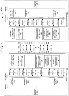
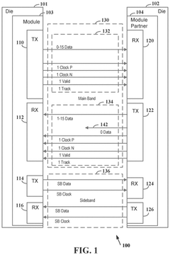
Interface conversion circuitry for universal chiplet interconnect express (UCIe)
PatentActiveUS12248419B1
Innovation
- The implementation of a converter circuit between the UCIe interface circuit and the bump interface, which includes local clock circuitry, oversampling circuitry, and majority detection circuitry, reduces the number of sideband links and corresponding bumps, thereby enhancing bandwidth density and reducing costs.
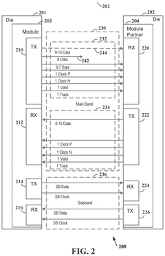
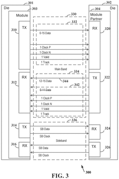
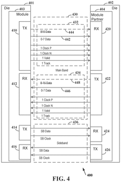
Variable link width in two directions for main band chip module connection
PatentPendingUS20240354279A1
Innovation
- Implementing a method to establish a die-to-die connection with a variable link width, allowing for independent configuration of transmit and receive data lanes through a sideband communication, enabling operation with different numbers of active data lanes in each direction to optimize power usage and data rates, and supporting fault tolerance by excluding faulty lines.
Standardization Efforts and Industry Collaboration
The UCIe (Universal Chiplet Interconnect Express) standardization process represents one of the most significant collaborative efforts in the semiconductor industry in recent years. The consortium behind UCIe has grown to include over 80 member companies spanning the entire ecosystem, from chip designers and manufacturers to packaging specialists and system integrators. This broad participation ensures that the standard addresses the needs of diverse stakeholders while promoting interoperability across different implementations.
The Interop Plugfest events have emerged as critical milestones in the standardization journey, providing a structured environment for companies to test their UCIe implementations against those from other vendors. These events have accelerated the maturation of the standard by identifying compatibility issues early in the development cycle, allowing for timely refinements to the specification before widespread commercial deployment.
Industry collaboration has been particularly evident in the working groups focused on specific aspects of the UCIe standard. These groups have tackled challenges related to physical layer design, protocol optimization, power management, and testing methodologies. The collaborative approach has enabled the integration of diverse expertise, resulting in a more robust and comprehensive standard than would have been possible through individual company efforts.
The standardization process has also benefited from the involvement of academic institutions and research organizations, which have contributed theoretical insights and experimental data to inform the development of the specification. This academic-industry partnership has helped address fundamental technical challenges while ensuring the standard remains grounded in practical implementation considerations.
Regulatory bodies and industry associations have played a supportive role in the UCIe standardization effort, providing frameworks for intellectual property management and ensuring alignment with broader industry initiatives. This coordination has been essential for navigating potential conflicts between competing interests and establishing a level playing field for all participants.
Looking forward, the lessons from the UCIe Interop Plugfest highlight the importance of maintaining open channels of communication among consortium members as the standard continues to evolve. The establishment of regular testing events, shared reference designs, and compliance certification programs will be crucial for sustaining the momentum of industry collaboration and ensuring the long-term success of the UCIe ecosystem.
Manufacturing and Integration Considerations
The manufacturing and integration of UCIe chiplet interconnect technology presents significant challenges that were highlighted during the recent Interop Plugfest events. The physical implementation of chiplet-based designs requires precise manufacturing processes to ensure reliable connections between different dies. Manufacturing tolerances become critical when dealing with the microbump arrays used in UCIe, which typically have pitches of 25-45μm. These fine-pitch interconnects demand extremely tight control over alignment, planarity, and material consistency.
Temperature management emerged as a key consideration during the Plugfest demonstrations. The thermal characteristics of multi-die packages differ substantially from traditional monolithic designs, requiring innovative approaches to heat dissipation. Thermal interface materials must be carefully selected to accommodate the varying expansion coefficients of different chiplets while maintaining effective heat transfer across the entire package.
Assembly processes for UCIe implementations require specialized equipment and techniques. The Plugfest revealed that pick-and-place accuracy for chiplet positioning needs to be within ±3μm to ensure proper connection. Additionally, the reflow process must be precisely controlled to prevent issues such as die shifting, voiding, or incomplete connections between the microbumps and landing pads.
Testing methodologies for UCIe-based systems present unique challenges compared to traditional integrated circuits. The Plugfest demonstrated the importance of developing standardized test protocols that can verify both the physical connections and the protocol-level functionality of the UCIe interface. Known-good-die testing becomes particularly important to avoid costly rework of assembled packages.
Supply chain considerations were also highlighted during the Plugfest. The successful implementation of UCIe technology requires close collaboration between foundries, OSAT providers, and system integrators. Standardization of manufacturing processes and quality control metrics across the supply chain is essential for the widespread adoption of chiplet-based designs.
Yield management strategies must evolve to accommodate the unique challenges of multi-die integration. The Plugfest demonstrated that defect density calculations need to account for both individual chiplet yields and the additional yield impact of the integration process itself. Statistical models presented at the event suggested that even small improvements in assembly yield can significantly impact overall economics of chiplet-based designs.
Unlock deeper insights with PatSnap Eureka Quick Research — get a full tech report to explore trends and direct your research. Try now!
Generate Your Research Report Instantly with AI Agent
Supercharge your innovation with PatSnap Eureka AI Agent Platform!