Precision Ultrafiltration in Semiconductor Manufacturing: Process Validation
SEP 22, 20259 MIN READ
Generate Your Research Report Instantly with AI Agent
Patsnap Eureka helps you evaluate technical feasibility & market potential.
Semiconductor Ultrafiltration Background and Objectives
Ultrafiltration technology has evolved significantly over the past four decades, becoming increasingly critical in semiconductor manufacturing processes. Initially developed for biological separations in the 1970s, ultrafiltration membranes have been progressively refined to meet the stringent purity requirements of semiconductor fabrication. The evolution from cellulose-based membranes to advanced polymer and ceramic composites has enabled filtration at the nanometer scale, essential for modern semiconductor processes.
The semiconductor industry's relentless pursuit of miniaturization, following Moore's Law, has driven the need for increasingly precise filtration technologies. As circuit features have shrunk from micrometers to nanometers, contamination control requirements have become exponentially more demanding. Even sub-nanometer particles can now cause critical defects in advanced semiconductor devices, necessitating ultrafiltration systems capable of removing contaminants at unprecedented levels of precision.
Current technological trends in semiconductor ultrafiltration focus on achieving higher flux rates while maintaining or improving rejection capabilities. Innovations in membrane materials, including the incorporation of nanostructured materials and surface modifications, are enabling more selective filtration with reduced fouling tendencies. Additionally, the integration of real-time monitoring systems and predictive analytics is transforming ultrafiltration from a passive to an intelligent process component.
The primary objective of precision ultrafiltration in semiconductor manufacturing is to ensure the removal of particles, macromolecules, and colloids that could compromise device yield and reliability. This includes eliminating contaminants from process chemicals, deionized water, and cleaning solutions used throughout the fabrication process. Beyond particle removal, modern ultrafiltration systems must also address dissolved contaminants and biological materials that can affect semiconductor performance.
Process validation represents a critical aspect of semiconductor ultrafiltration, ensuring that filtration systems consistently deliver the required performance under actual manufacturing conditions. This involves establishing robust protocols for membrane integrity testing, filtration efficiency verification, and long-term performance monitoring. The validation process must account for variations in feed composition, operating conditions, and membrane aging to guarantee consistent results.
Looking forward, the industry aims to develop ultrafiltration technologies capable of supporting next-generation semiconductor processes, including extreme ultraviolet (EUV) lithography and 3D integration. These advanced manufacturing techniques require even higher levels of purity and process control, pushing ultrafiltration technology toward molecular-level selectivity and real-time adaptability to changing process conditions.
Market Requirements for High-Purity Process Fluids
The semiconductor industry's demand for high-purity process fluids has intensified dramatically with the continued miniaturization of integrated circuits and the increasing complexity of semiconductor manufacturing processes. As node sizes shrink below 5nm, even nanoscale contaminants can significantly impact yield rates and device performance. This has created stringent requirements for ultrapure water (UPW) and chemical solutions used throughout the fabrication process.
Current market specifications demand process fluids with contamination levels in the parts-per-trillion (ppt) range, with particular emphasis on the removal of particles, dissolved metals, organic compounds, and microbial contaminants. Leading semiconductor manufacturers require total organic carbon (TOC) levels below 1 ppb and particle counts approaching zero for critical processes. These requirements continue to tighten as manufacturing processes evolve toward 3nm and 2nm nodes.
The economic implications of these purity requirements are substantial. The global market for high-purity chemicals in semiconductor manufacturing exceeded $5 billion in 2022, with projected annual growth rates of 8-10% through 2028. Ultrapure water systems represent another significant segment, with installations costing between $20-100 million for advanced fabrication facilities.
Beyond purity levels, consistency and reliability have emerged as equally critical market requirements. Semiconductor manufacturers demand process fluids with minimal batch-to-batch variations to ensure reproducible manufacturing outcomes. This has driven the need for advanced real-time monitoring systems and process validation protocols that can verify fluid purity throughout the manufacturing process.
Sustainability considerations are increasingly influencing market requirements as well. The semiconductor industry faces mounting pressure to reduce water consumption and chemical waste. Advanced ultrafiltration systems that enable higher recovery rates and recycling of process fluids are gaining traction, with manufacturers willing to invest in technologies that balance purity requirements with environmental considerations.
Regional variations in requirements exist, with facilities in water-stressed regions like Taiwan and Arizona placing greater emphasis on water recycling capabilities. Meanwhile, facilities in regions with stricter environmental regulations, such as Europe and parts of East Asia, prioritize systems with reduced chemical waste and lower environmental footprints.
The market increasingly demands integrated solutions that combine precision ultrafiltration with comprehensive validation protocols. This trend reflects the industry's move toward more automated, data-driven manufacturing environments where process fluid purity is continuously monitored and validated rather than periodically tested.
Ultrafiltration Technology Landscape and Barriers
Ultrafiltration technology in semiconductor manufacturing has evolved significantly over the past decades, transitioning from basic filtration methods to highly sophisticated precision systems. The current landscape is characterized by membrane-based technologies capable of removing particles down to 0.001-0.1 microns, essential for ultra-pure water production in advanced semiconductor processes. These systems typically operate at pressures between 2-10 bar and achieve flow rates optimized for semiconductor manufacturing requirements.
The global market for ultrafiltration in semiconductor manufacturing is dominated by cross-flow and dead-end filtration configurations, with hollow fiber and spiral wound membrane modules being the most prevalent designs. Polymeric membranes, particularly polysulfone, polyethersulfone, and PVDF, represent approximately 75% of installations, while ceramic membranes are gaining traction for specialized applications requiring extreme chemical or thermal resistance.
Despite technological advancements, significant barriers persist in ultrafiltration implementation for semiconductor manufacturing. Membrane fouling remains the primary challenge, reducing filtration efficiency and increasing operational costs. Current anti-fouling strategies include chemical cleaning protocols, backwashing systems, and surface modifications, yet these solutions often introduce complexity and potential chemical contamination risks to the ultrapure water system.
Precision validation presents another substantial barrier, as semiconductor manufacturing requires increasingly stringent filtration standards with each technology node advancement. Current validation methodologies struggle to consistently detect contaminants at sub-nanometer scales, creating a technological gap between filtration capabilities and verification requirements. This validation challenge is particularly acute for particles in the 10-100nm range, where detection reliability diminishes significantly.
Energy consumption represents a growing concern, with ultrafiltration systems typically accounting for 15-20% of water purification energy costs in semiconductor facilities. The trade-off between filtration precision and energy efficiency creates implementation barriers, particularly for facilities transitioning to more advanced manufacturing processes.
Regulatory compliance adds another layer of complexity, with different regions implementing varying standards for ultrapure water quality and waste discharge. This regulatory fragmentation creates barriers to standardized ultrafiltration implementation across global semiconductor manufacturing networks, forcing customization that increases costs and complicates validation protocols.
Material limitations also constrain ultrafiltration advancement, as membrane materials with ideal chemical resistance often lack the mechanical strength needed for high-pressure applications, while mechanically robust materials may introduce contamination risks through leaching or degradation. This materials science challenge represents a fundamental barrier to achieving the perfect balance of filtration precision, durability, and purity required for next-generation semiconductor manufacturing.
Current Ultrafiltration Validation Methodologies
01 Validation protocols for ultrafiltration processes
Validation protocols are essential for ensuring the reliability and consistency of ultrafiltration processes. These protocols involve establishing acceptance criteria, defining critical process parameters, and implementing systematic testing procedures. Validation includes performance qualification, operational qualification, and installation qualification phases to verify that the ultrafiltration system consistently meets predetermined specifications under normal operating conditions.- Validation protocols for ultrafiltration processes: Validation protocols are essential for ensuring the reliability and consistency of ultrafiltration processes. These protocols involve establishing acceptance criteria, defining critical process parameters, and implementing monitoring systems to verify that the ultrafiltration process consistently meets predetermined specifications. Validation includes installation qualification (IQ), operational qualification (OQ), and performance qualification (PQ) to ensure the system operates as intended under actual processing conditions.
- Membrane integrity testing and monitoring systems: Membrane integrity testing is crucial for precision ultrafiltration validation. This involves implementing automated monitoring systems that can detect membrane defects, leaks, or performance degradation in real-time. Advanced sensors and analytical tools are used to continuously monitor parameters such as pressure differentials, flow rates, and filtrate quality. These monitoring systems help ensure the ultrafiltration process maintains its specified separation efficiency and prevents contamination of the filtrate.
- Process parameter optimization and control strategies: Optimizing and controlling process parameters is essential for ultrafiltration validation. This involves establishing acceptable ranges for critical parameters such as transmembrane pressure, cross-flow velocity, temperature, and pH. Statistical process control methods are implemented to maintain these parameters within validated ranges. Automated control systems with feedback loops adjust operating conditions in real-time to ensure consistent filtration performance and product quality throughout the process.
- Cleaning and sanitization validation procedures: Validation of cleaning and sanitization procedures is critical for maintaining ultrafiltration system performance and preventing cross-contamination. This involves developing and validating protocols for chemical cleaning, disinfection, and sterilization of membrane systems. Validation includes verification of cleaning agent effectiveness, determination of residual cleaning agent limits, and establishment of cleaning cycle parameters. Regular testing confirms the removal of process residues, microbial contaminants, and cleaning agents to ensure membrane longevity and product purity.
- Data management and documentation systems: Comprehensive data management and documentation systems are essential components of ultrafiltration process validation. These systems capture, store, and analyze process data, validation test results, and quality control measurements. Electronic records management ensures data integrity, traceability, and compliance with regulatory requirements. Documentation includes validation master plans, protocols, test results, deviation reports, and change control procedures that demonstrate the validated state of the ultrafiltration process throughout its lifecycle.
02 Membrane integrity testing and monitoring systems
Membrane integrity testing is crucial for validating ultrafiltration processes. Advanced monitoring systems can detect microscopic defects in membranes that might compromise filtration efficiency. These systems employ various techniques such as pressure decay tests, bubble point tests, and continuous monitoring of transmembrane pressure to ensure membrane integrity throughout the filtration process. Real-time monitoring allows for immediate detection of membrane failures and ensures product quality.Expand Specific Solutions03 Data management and analytical methods for process validation
Effective data management systems and analytical methods are essential components of ultrafiltration process validation. These systems collect, store, and analyze process data to verify that the ultrafiltration process consistently operates within established parameters. Statistical process control methods are employed to identify trends and deviations, while validation software platforms facilitate documentation and compliance with regulatory requirements. Advanced analytics help in establishing correlations between process parameters and filtration outcomes.Expand Specific Solutions04 Critical process parameters and control strategies
Identification and control of critical process parameters are fundamental to ultrafiltration process validation. Parameters such as transmembrane pressure, flow rate, temperature, pH, and conductivity significantly impact filtration efficiency and product quality. Establishing acceptable ranges for these parameters and implementing robust control strategies ensures consistent performance of the ultrafiltration system. Process analytical technology can be integrated to provide real-time monitoring and adjustment of these critical parameters.Expand Specific Solutions05 Cleaning and sanitization validation for ultrafiltration systems
Validation of cleaning and sanitization procedures is essential for maintaining the performance and longevity of ultrafiltration systems. This involves establishing protocols to verify the removal of process residues, contaminants, and microbial biofilms from membrane surfaces and associated equipment. Validation methods include visual inspection, rinse water analysis, swab testing, and microbial testing to ensure that cleaning procedures effectively restore the system to a predetermined state of cleanliness and sterility.Expand Specific Solutions
Leading Semiconductor Filtration Solution Providers
The precision ultrafiltration market in semiconductor manufacturing is currently in a growth phase, with increasing demand driven by miniaturization trends and higher purity requirements. The market is expected to reach significant scale as semiconductor fabrication processes become more sophisticated. Technologically, companies like Taiwan Semiconductor Manufacturing Co. and Samsung Electronics are leading innovation with advanced filtration validation protocols, while Applied Materials Israel and GlobalFoundries are developing specialized equipment for ultrafiltration process control. IBM and Renesas Electronics are focusing on integration of ultrafiltration with AI-based monitoring systems. Asian manufacturers, particularly SMIC and KIOXIA, are rapidly advancing their capabilities to compete with established players. The technology is approaching maturity in leading fabs but continues to evolve with new materials and process requirements.
Applied Materials Israel Ltd.
Technical Solution: Applied Materials has developed an advanced precision ultrafiltration system specifically designed for semiconductor manufacturing processes. Their solution integrates real-time monitoring capabilities with automated process validation protocols. The system employs multi-stage filtration architecture with sub-nanometer precision filters capable of removing particles down to 10nm size. Their proprietary CMP (Chemical Mechanical Planarization) slurry filtration technology incorporates advanced membrane materials that maintain consistent pore size distribution even under varying pressure conditions. The system features in-situ contamination detection using laser scattering techniques that can identify defects in real-time without interrupting the manufacturing process. Applied Materials' validation methodology includes automated statistical process control that continuously monitors filter performance parameters and provides predictive maintenance alerts before failures occur, significantly reducing unexpected downtime.
Strengths: Superior particle removal efficiency with documented 99.9999% filtration effectiveness for particles >20nm. Integrated validation system reduces manual testing requirements by approximately 70%. Weaknesses: Higher initial implementation cost compared to conventional filtration systems. Requires specialized training for operators to fully utilize the advanced monitoring capabilities.
Taiwan Semiconductor Manufacturing Co., Ltd.
Technical Solution: TSMC has pioneered a comprehensive precision ultrafiltration validation framework for their advanced semiconductor manufacturing processes. Their approach combines physical filtration with chemical purification techniques optimized for different process steps. The company employs a multi-tiered filtration strategy with dedicated systems for critical areas such as photolithography, wet etching, and CMP processes. For their most advanced nodes (5nm and below), TSMC utilizes custom-designed ceramic membrane filters with precisely controlled pore size distribution. Their validation protocol incorporates both online and offline monitoring systems, with automated sampling at multiple points in the production line. TSMC's process validation methodology includes continuous particle counting, resistivity measurements, and TOC (Total Organic Carbon) analysis to ensure ultrapure water quality meets their stringent specifications. The company has developed proprietary software algorithms that correlate filtration parameters with final yield data, enabling predictive maintenance and process optimization.
Strengths: Highly integrated approach that connects filtration performance directly to yield metrics, allowing for data-driven optimization. Demonstrated ability to maintain consistent filtration performance across high-volume manufacturing environments. Weaknesses: System complexity requires significant engineering resources for implementation and maintenance. Highly customized solutions may limit transferability to different manufacturing contexts.
Critical Patents in Semiconductor Filtration Validation
Method for producing ultrapure water, ultrapure water production apparatus, and ultrapure water production system
PatentPendingUS20250263313A1
Innovation
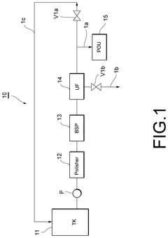
- A method involving filtration through ultrafiltration, microfiltration, or ion exchange membranes under specific conditions, including a permeate water flux between 0.5 to 2.0 times the optimum flux and a water recovery rate of 50% to 80%, to effectively reduce iron and silica concentrations without complex equipment.
System for trapping fine particles in ultra-pure water and method for measuring fine particle density
PatentWO2012073594A1
Innovation
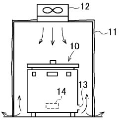
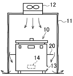
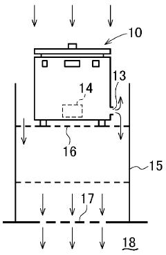
- A centrifugal filtration system with a partition member or guide member is implemented to prevent motor exhaust from contaminating the centrifugal filtration device, ensuring that fine particles from the exhaust are filtered out, and a method for measuring fine particle concentration by counting trapped particles on the filter with high accuracy.
Contamination Risk Assessment Framework
The development of a comprehensive Contamination Risk Assessment Framework is essential for precision ultrafiltration processes in semiconductor manufacturing. This framework must systematically identify, evaluate, and mitigate potential contamination sources that could compromise wafer integrity and device performance. The framework begins with a detailed mapping of the entire ultrafiltration process, identifying critical control points where contamination risks are highest, such as filter interfaces, fluid transfer points, and storage systems.
Risk categorization forms the second component, classifying contaminants based on their physical properties (particulate, ionic, organic) and potential impact severity. This classification enables prioritization of mitigation efforts toward the most critical risk factors. Semiconductor manufacturing demands exceptional purity levels, with even nanoscale contaminants potentially causing catastrophic device failures.
Quantitative assessment methodologies constitute the third framework element, incorporating statistical process control techniques to establish baseline contamination levels and acceptable variation thresholds. These methodologies typically employ advanced analytical tools such as scanning electron microscopy, mass spectrometry, and particle counters to detect contaminants at parts-per-trillion levels.
The framework further integrates real-time monitoring protocols that utilize in-line sensors and automated sampling systems to provide continuous contamination surveillance. These systems generate alerts when measurements approach predefined thresholds, enabling proactive intervention before contamination events occur. This capability is particularly valuable during process validation phases when establishing operational parameters.
Mitigation strategy development represents another critical framework component, outlining standardized response procedures for different contamination scenarios. These strategies include immediate actions (process shutdown, system purging) and long-term preventive measures (filter redesign, material substitution). The framework emphasizes a hierarchical approach to contamination control, prioritizing elimination of contamination sources over filtration or remediation.
Documentation and traceability systems form the final framework element, maintaining comprehensive records of all contamination events, mitigation actions, and validation results. This historical database supports trend analysis and continuous improvement initiatives while satisfying regulatory compliance requirements. The framework's effectiveness ultimately depends on its integration with broader quality management systems and regular updates based on emerging contamination challenges in increasingly sophisticated semiconductor manufacturing processes.
Regulatory Compliance for Semiconductor Manufacturing
Semiconductor manufacturing operates within a complex regulatory landscape that demands strict adherence to multiple standards and compliance frameworks. For precision ultrafiltration processes, regulatory compliance is not merely a legal obligation but a critical quality assurance mechanism that ensures product integrity and market access.
The semiconductor industry must navigate regulations from various international bodies, including the International Organization for Standardization (ISO), particularly ISO 14644 for cleanroom standards and ISO 9001 for quality management systems. These standards establish the baseline requirements for contamination control in ultrafiltration processes, defining acceptable particulate levels and validation methodologies.
Environmental regulations present another significant compliance dimension, with frameworks such as the Restriction of Hazardous Substances (RoHS) and Registration, Evaluation, Authorization and Restriction of Chemicals (REACH) governing the materials and chemicals used in semiconductor manufacturing. Ultrafiltration processes must be designed to minimize environmental impact while maintaining process efficiency, often requiring specialized waste management protocols and chemical handling procedures.
Process validation for precision ultrafiltration must also comply with industry-specific standards such as SEMI (Semiconductor Equipment and Materials International) guidelines. SEMI F57, for instance, provides protocols for ultrapure water systems used in semiconductor manufacturing, directly impacting ultrafiltration process design and validation requirements.
Documentation requirements represent a substantial aspect of regulatory compliance, with manufacturers needing to maintain comprehensive records of process validation activities, equipment calibration, maintenance logs, and personnel training. These records must be readily accessible during regulatory inspections and audits, necessitating robust document management systems.
Regional variations in regulatory requirements add complexity to global semiconductor operations. While the European Union emphasizes environmental protection through directives like REACH, countries like Japan focus on precision manufacturing standards through the Japan Electronics and Information Technology Industries Association (JEITA) guidelines. The United States, through agencies such as the Environmental Protection Agency (EPA) and Occupational Safety and Health Administration (OSHA), places significant emphasis on worker safety and environmental protection in manufacturing processes.
Emerging regulations around nanomaterials and ultrafine particles are increasingly relevant to precision ultrafiltration, as regulatory bodies worldwide develop frameworks to address potential risks associated with nanoscale manufacturing processes. Manufacturers must stay vigilant about these evolving requirements to ensure continued compliance.
Unlock deeper insights with Patsnap Eureka Quick Research — get a full tech report to explore trends and direct your research. Try now!
Generate Your Research Report Instantly with AI Agent
Supercharge your innovation with Patsnap Eureka AI Agent Platform!
