

Nickel Molybdenum Alloy Heat Exchanger Material: Comprehensive Analysis Of Composition, Performance, And Industrial Applications
JUL 16, 20259 MIN READ
Generate Your Research Report Instantly with AI Agent
PatSnap Eureka helps you evaluate technical feasibility & market potential.
Chiplet Evolution and Objectives
Chiplet technology has emerged as a revolutionary approach in the semiconductor industry, addressing the challenges of traditional monolithic chip designs. The evolution of chiplets can be traced back to the early 2010s when the limitations of Moore's Law became increasingly apparent. As transistor scaling slowed down, chip designers sought alternative methods to improve performance and reduce costs.
The primary objective of chiplet architecture is to enable modular computing by breaking down complex system-on-chip (SoC) designs into smaller, more manageable components. This approach allows for greater flexibility in chip design, improved yield, and the ability to mix and match different process nodes within a single package. By leveraging advanced packaging technologies, such as 2.5D and 3D integration, chiplets can be interconnected to form high-performance, power-efficient systems.
One of the key milestones in chiplet evolution was the introduction of AMD's Zen-based processors in 2017, which utilized a multi-chip module (MCM) design. This approach demonstrated the viability of chiplet architecture in mainstream computing products. Since then, other major players in the semiconductor industry, including Intel and TSMC, have embraced chiplet technology and developed their own implementations.
The evolution of chiplets has been driven by several factors, including the need for improved performance, reduced power consumption, and enhanced scalability. As traditional monolithic designs reached their limits, chiplets offered a way to continue advancing semiconductor technology while managing costs and complexity. The modular nature of chiplets also allows for greater customization and faster time-to-market for new products.
Looking ahead, the objectives of chiplet technology are multifaceted. One primary goal is to establish industry-wide standards for chiplet interfaces and packaging, enabling greater interoperability between different vendors' components. This standardization effort, led by initiatives such as the Universal Chiplet Interconnect Express (UCIe) consortium, aims to create a more open and flexible ecosystem for modular computing.
Another key objective is to push the boundaries of chiplet integration, exploring new packaging technologies and interconnect solutions. This includes advancements in through-silicon vias (TSVs), silicon interposers, and hybrid bonding techniques to achieve higher bandwidth and lower latency between chiplets. Additionally, researchers are investigating novel materials and manufacturing processes to further enhance chiplet performance and efficiency.
As chiplet technology continues to evolve, its role in modular computing is expected to expand beyond traditional processor and memory applications. Future objectives include integrating diverse components such as analog/RF circuits, photonics, and specialized accelerators into chiplet-based systems. This heterogeneous integration will enable highly customized solutions for emerging applications in artificial intelligence, edge computing, and high-performance computing.
Market Demand Analysis
The market demand for chiplet architecture and modular computing solutions has been steadily increasing in recent years, driven by the growing need for more powerful and efficient computing systems across various industries. As traditional monolithic chip designs approach their physical limits, chiplet-based architectures offer a promising alternative to meet the ever-increasing performance requirements of modern applications.
In the data center and cloud computing sector, there is a significant demand for high-performance, energy-efficient processors that can handle complex workloads such as artificial intelligence, machine learning, and big data analytics. Chiplet architecture allows for the integration of specialized processing units, memory, and I/O components, enabling customized solutions that can be tailored to specific workload requirements. This flexibility is particularly attractive to cloud service providers and enterprise customers seeking to optimize their infrastructure for diverse applications.
The telecommunications industry is another key driver of market demand for chiplet-based solutions. With the ongoing rollout of 5G networks and the anticipated transition to 6G in the future, there is a growing need for advanced networking equipment capable of handling increased data throughput and lower latency requirements. Chiplet architecture enables the development of more powerful and efficient network processors and base station equipment, supporting the evolution of mobile communication technologies.
In the consumer electronics market, chiplet technology is gaining traction as manufacturers seek to deliver more powerful and feature-rich devices within constrained form factors and power envelopes. Smartphones, tablets, and laptops can benefit from chiplet-based designs that integrate high-performance CPU cores, graphics processors, and specialized AI accelerators while maintaining energy efficiency.
The automotive industry is also showing increased interest in chiplet architecture as vehicles become more connected and autonomous. Advanced driver assistance systems (ADAS) and infotainment systems require sophisticated computing platforms that can process vast amounts of sensor data in real-time. Chiplet-based solutions offer the potential to create scalable and adaptable automotive computing platforms that can meet the evolving needs of the industry.
The market for chiplet technology is expected to grow significantly in the coming years. Industry analysts project that the global chiplet market will experience double-digit compound annual growth rates over the next decade. This growth is driven by the increasing adoption of chiplet-based designs across multiple sectors, including high-performance computing, edge computing, and consumer electronics.
As the demand for more powerful and efficient computing solutions continues to rise, chiplet architecture and modular computing are poised to play a crucial role in shaping the future of semiconductor design and manufacturing. The ability to mix and match different chiplets to create customized solutions offers unprecedented flexibility and scalability, making it an attractive option for a wide range of applications and industries.
Chiplet Tech Challenges
Despite the promising potential of chiplet architecture in modular computing, several significant technical challenges persist. One of the primary obstacles is the interconnect technology between chiplets. As the number of chiplets increases, the complexity of interconnections grows exponentially, leading to potential bottlenecks in data transfer and increased power consumption. Developing high-bandwidth, low-latency, and energy-efficient interconnect solutions remains a critical challenge.
Another major hurdle is thermal management. With multiple chiplets packed closely together, heat dissipation becomes a significant concern. Uneven heat distribution can lead to hotspots, potentially causing performance degradation or even system failures. Innovative cooling solutions and thermal design techniques are necessary to address this issue effectively.
The integration and packaging of chiplets present another set of challenges. As chiplets become smaller and more numerous, precise alignment and bonding techniques are crucial. Advanced packaging technologies, such as 2.5D and 3D integration, require sophisticated manufacturing processes and materials, which can increase production costs and complexity.
Standardization is yet another challenge in the chiplet ecosystem. The lack of universal standards for chiplet interfaces and protocols hinders interoperability between chiplets from different manufacturers. This fragmentation can limit the flexibility and modularity that chiplet architecture promises to deliver.
Power management across multiple chiplets is also a significant concern. Coordinating power delivery and optimizing power consumption across various chiplets with different performance characteristics and power requirements is a complex task. Developing efficient power management strategies that can dynamically adjust to varying workloads and thermal conditions is crucial for maximizing the benefits of chiplet architecture.
Testing and validation of chiplet-based systems present unique challenges. Traditional testing methods may not be sufficient for complex multi-chiplet designs. Developing new testing methodologies and tools that can effectively verify the functionality and performance of interconnected chiplets is essential for ensuring reliability and quality.
Lastly, the design and optimization of software to fully leverage the potential of chiplet architecture is a significant challenge. Existing software frameworks and algorithms may not be optimized for the distributed nature of chiplet-based systems. Developing new programming models and tools that can efficiently utilize the modular and heterogeneous nature of chiplet architectures is crucial for realizing their full potential in various computing applications.
Current Chiplet Solutions
01 Chiplet interconnection and integration
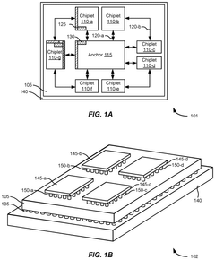
Chiplet architecture focuses on interconnecting multiple smaller chips (chiplets) to form a larger, more complex system. This approach allows for improved performance, power efficiency, and scalability. The integration involves advanced packaging technologies and high-speed interconnects to enable communication between chiplets.- Chiplet interconnection and integration: Chiplet architecture focuses on interconnecting multiple smaller chips (chiplets) to form a larger, more complex system. This approach allows for better yield, flexibility, and cost-effectiveness in semiconductor manufacturing. The integration involves advanced packaging technologies and high-speed interconnects to ensure efficient communication between chiplets.
- 3D stacking and heterogeneous integration: Chiplet architectures often employ 3D stacking techniques to vertically integrate different chiplets. This allows for heterogeneous integration of various components, such as processors, memory, and I/O interfaces, in a single package. The approach enables higher performance, reduced power consumption, and smaller form factors.
- Interposer and substrate technologies: Advanced interposer and substrate technologies play a crucial role in chiplet architectures. These components provide the necessary interconnections between chiplets and facilitate power delivery and signal routing. Silicon interposers and organic substrates are commonly used to support high-density connections and manage thermal dissipation.
- Power management and thermal solutions: Efficient power management and thermal solutions are essential in chiplet architectures due to the high-density integration of multiple components. This includes advanced power delivery networks, on-chip voltage regulators, and innovative cooling solutions to maintain optimal performance and reliability of the integrated system.
- Design and verification methodologies: Chiplet architectures require specialized design and verification methodologies to ensure proper functionality and performance of the integrated system. This includes advanced EDA tools, simulation techniques, and testing strategies to address challenges such as signal integrity, timing closure, and thermal management across multiple chiplets.
02 3D stacking and through-silicon vias (TSVs)
3D stacking of chiplets is a key aspect of advanced chiplet architectures. This technique involves vertically stacking multiple chiplets and using through-silicon vias (TSVs) for inter-layer connections. 3D stacking allows for higher density, reduced footprint, and improved performance in chiplet-based systems.Expand Specific Solutions03 Heterogeneous integration of chiplets
Chiplet architecture enables the integration of different types of chips, each optimized for specific functions. This heterogeneous integration allows for combining chips manufactured using different process nodes or technologies, leading to improved overall system performance and cost-effectiveness.Expand Specific Solutions04 Power management and thermal considerations
Efficient power management and thermal control are crucial in chiplet architectures. This includes techniques for dynamic power gating, voltage scaling, and thermal management across multiple chiplets. Advanced cooling solutions and power distribution networks are designed to address the unique challenges of chiplet-based systems.Expand Specific Solutions05 Chiplet design and verification methodologies
Developing effective design and verification methodologies is essential for chiplet-based systems. This includes creating standardized interfaces, ensuring interoperability between chiplets from different vendors, and developing tools and processes for system-level verification and testing of chiplet-based architectures.Expand Specific Solutions
Key Chiplet Players
The chiplet architecture and modular computing market is in a growth phase, with increasing adoption across the semiconductor industry. The market size is expanding rapidly, driven by demand for more efficient and scalable computing solutions. Technologically, chiplets are maturing but still evolving, with key players like Intel, AMD, and Qualcomm investing heavily in research and development. Companies such as Micron and Applied Materials are also contributing to the ecosystem. While established semiconductor giants lead the way, startups like D-Matrix and MemryX are bringing innovative approaches to chiplet design and integration. The competitive landscape is dynamic, with both collaboration and competition shaping the future of modular computing architectures.
Intel Corp.
Technical Solution: Intel's chiplet architecture, known as "Foveros," utilizes 3D packaging technology to stack multiple chiplets vertically[1]. This approach allows for the integration of diverse IP blocks and process nodes within a single package. Intel's Meteor Lake processors, for instance, employ chiplets for the CPU, GPU, and I/O, manufactured on different process nodes[2]. The company has also introduced advanced interconnect technologies like EMIB (Embedded Multi-die Interconnect Bridge) to enable high-bandwidth, low-latency communication between chiplets[3]. Intel's research focuses on optimizing die-to-die interfaces, thermal management, and power delivery in multi-chiplet designs[4].
Strengths: Advanced 3D packaging technology, diverse IP integration, and established manufacturing capabilities. Weaknesses: Potential thermal challenges in 3D stacked designs and complexity in coordinating multiple process nodes.
Xilinx, Inc.
Technical Solution: Xilinx, now part of AMD, has been at the forefront of chiplet technology in the FPGA domain. The company's Versal ACAP (Adaptive Compute Acceleration Platform) architecture utilizes a modular approach, combining FPGA fabric, ARM CPU cores, and AI engines in a single package[12]. Xilinx's research focuses on developing high-bandwidth, low-latency interconnects between chiplets, such as their proprietary SSIT (Stacked Silicon Interconnect Technology)[13]. The company is also exploring the integration of HBM (High Bandwidth Memory) as separate chiplets in their high-performance FPGA designs[14]. Xilinx's approach to chiplet architecture aims to provide flexible, customizable solutions for diverse applications in data centers, edge computing, and telecommunications.
Strengths: Expertise in programmable logic, flexible and customizable designs, and integration of heterogeneous compute elements. Weaknesses: Potential complexity in programming and optimizing heterogeneous systems, and higher costs compared to ASIC solutions.
Core Chiplet Innovations
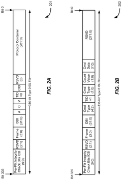
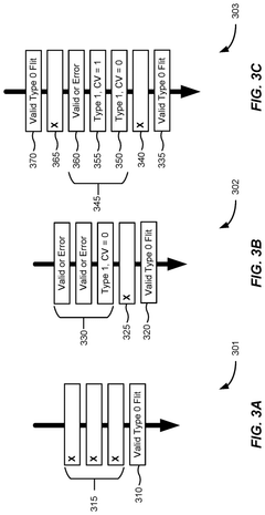
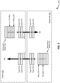
System-level techniques for error correction in chip-to-chip interfaces
PatentPendingUS20250030500A1
Innovation
- A retry-based error correction mechanism is implemented for chip-to-chip interfaces, which includes encoding data Flits to transmit control Flits, reducing the need for extra control signals, and utilizing Type-0 and Type-1 Flits for data and control messages respectively, with a retransmission mode triggered by error detection.
Modular GPU architecture for clients and servers
PatentPendingIN202244051173A
Innovation
- A modular and scalable system-on-a-chip (SoC) architecture is introduced, allowing for the selection of various modules based on memory technology and intended use cases, enabling the creation of discrete graphics processing units that can be packaged into different product classes and market segments, thereby optimizing performance across clients and servers.
Chiplet Ecosystem Impact
The Chiplet ecosystem has emerged as a transformative force in the semiconductor industry, reshaping the landscape of chip design, manufacturing, and integration. This modular approach to chip architecture has far-reaching implications across the entire value chain, from design houses to foundries and packaging specialists.
At the core of the Chiplet ecosystem is the concept of disaggregation, which allows for the separation of complex system-on-chip (SoC) designs into smaller, more manageable components. This paradigm shift has opened up new possibilities for collaboration and specialization within the industry. Design houses can now focus on their core competencies, creating highly optimized Chiplets for specific functions, while relying on integration partners to assemble these components into complete solutions.
The impact on manufacturing is equally significant. Foundries can now produce a wider range of products by combining different Chiplets, potentially improving yield rates and reducing costs. This flexibility allows for more efficient use of manufacturing capacity and enables faster time-to-market for new products. Additionally, the Chiplet approach aligns well with advanced packaging technologies, driving innovation in areas such as 2.5D and 3D integration.
The ecosystem has also fostered the development of new standards and interfaces, such as the Universal Chiplet Interconnect Express (UCIe), which aims to ensure interoperability between Chiplets from different vendors. This standardization effort is crucial for the long-term viability of the Chiplet model, as it enables a more open and competitive marketplace.
From a business perspective, the Chiplet ecosystem is reshaping competitive dynamics within the semiconductor industry. It lowers barriers to entry for smaller, specialized players who can now contribute innovative Chiplet designs without the need to develop entire SoCs. This democratization of chip design has the potential to accelerate innovation and diversify the market.
However, the transition to a Chiplet-based model is not without challenges. Issues such as thermal management, power distribution, and signal integrity become more complex in multi-die packages. The industry is actively working on solutions to these technical hurdles, driving advancements in materials science, packaging technologies, and design tools.
Looking ahead, the Chiplet ecosystem is poised to play a crucial role in addressing the increasing demand for specialized, high-performance computing solutions. As applications in artificial intelligence, edge computing, and 5G continue to evolve, the flexibility and scalability offered by Chiplet architectures will become increasingly valuable. This ecosystem approach may well be the key to sustaining Moore's Law-like advancements in the post-Moore's Law era.
Chiplet Design Standards
Chiplet design standards play a crucial role in the development and implementation of modular computing architectures. These standards ensure interoperability, consistency, and efficiency across different chiplet designs, enabling seamless integration and communication between various components within a system.
One of the primary chiplet design standards is the Advanced Interface Bus (AIB), developed by Intel. AIB provides a standardized interface for high-bandwidth, low-latency communication between chiplets. It supports both die-to-die and package-to-package connections, offering flexibility in system design. The AIB standard defines electrical and physical specifications, including signal integrity requirements and power management protocols, to ensure reliable data transfer between chiplets.
Another significant standard is the Universal Chiplet Interconnect Express (UCIe), which aims to create an open ecosystem for chiplet-based designs. UCIe builds upon the PCI Express (PCIe) standard, extending its capabilities to support die-to-die interconnects. This standard defines both the physical layer and protocol layer specifications, enabling high-speed communication between chiplets from different vendors.
The Open Compute Project (OCP) has also contributed to chiplet design standards through its Open Domain-Specific Architecture (ODSA) subproject. ODSA focuses on developing open interfaces and protocols for chiplet-based systems, promoting interoperability and reducing design complexity. The ODSA Bunch of Wires (BoW) interface is one such standard, providing a simple and cost-effective solution for chiplet interconnects.
Chiplet design standards also address thermal management and power distribution challenges. The Joint Electron Device Engineering Council (JEDEC) has developed standards for thermal interface materials and power delivery networks specifically tailored for chiplet-based designs. These standards ensure efficient heat dissipation and stable power supply across multiple chiplets within a package.
Standardization efforts extend to packaging technologies as well. The Heterogeneous Integration Roadmap (HIR), supported by IEEE, SEMI, and other industry organizations, provides guidelines for advanced packaging techniques suitable for chiplet integration. These standards cover aspects such as through-silicon vias (TSVs), interposers, and advanced substrate technologies.
As chiplet architectures continue to evolve, ongoing efforts are focused on developing standards for chiplet-to-chiplet authentication and security protocols. These standards aim to address potential vulnerabilities in multi-vendor chiplet ecosystems and ensure the integrity of data exchange between chiplets.
Unlock deeper insights with PatSnap Eureka Quick Research — get a full tech report to explore trends and direct your research. Try now!
Generate Your Research Report Instantly with AI Agent
Supercharge your innovation with PatSnap Eureka AI Agent Platform!