Chiplet Architecture and Its Role in Transformative Technological Solutions
JUL 16, 20259 MIN READ
Generate Your Research Report Instantly with AI Agent
Patsnap Eureka helps you evaluate technical feasibility & market potential.
Chiplet Evolution and Objectives
Chiplet architecture represents a paradigm shift in semiconductor design, evolving from traditional monolithic integrated circuits to a more modular and flexible approach. This evolution began in the early 2010s as a response to the increasing challenges of scaling traditional chip designs. The primary objective of chiplet technology is to overcome the limitations of Moore's Law by enabling the integration of multiple smaller dies, or "chiplets," onto a single package.
The development of chiplet architecture has been driven by several key factors. Firstly, the rising costs and technical difficulties associated with manufacturing large, complex chips on advanced process nodes have made traditional monolithic designs less economically viable. Chiplets allow for the combination of different process technologies within a single package, optimizing performance and cost. Secondly, the increasing demand for specialized computing solutions in areas such as artificial intelligence, high-performance computing, and edge devices has necessitated more flexible and customizable chip designs.
The evolution of chiplet technology can be traced through several significant milestones. In 2015, AMD introduced its Fiji GPU, which incorporated High Bandwidth Memory (HBM) as separate dies alongside the GPU, marking an early adoption of multi-chip module design. This was followed by Intel's announcement of its Embedded Multi-die Interconnect Bridge (EMIB) technology in 2017, facilitating high-speed connections between chiplets. AMD's launch of its Zen 2 architecture in 2019, utilizing a chiplet-based design for its Ryzen processors, demonstrated the potential for chiplets in mainstream consumer products.
As the technology has matured, industry standards have emerged to facilitate interoperability and accelerate adoption. The development of the Universal Chiplet Interconnect Express (UCIe) standard in 2022 represents a significant step towards creating an open ecosystem for chiplet-based designs. This standardization aims to enable chiplets from different manufacturers to work seamlessly together, fostering innovation and competition in the semiconductor industry.
Looking forward, the objectives of chiplet architecture are multifaceted. One primary goal is to continue pushing the boundaries of performance and efficiency in computing systems. By allowing for the optimal combination of different process nodes and specialized functions, chiplet designs can deliver tailored solutions for specific applications while maintaining cost-effectiveness. Another objective is to enhance scalability and flexibility in chip design, enabling rapid customization and reducing time-to-market for new products.
Furthermore, chiplet technology aims to address sustainability concerns in the semiconductor industry. By enabling the reuse of proven IP blocks and reducing the need for entire chip redesigns, chiplet architecture can potentially lower development costs and minimize electronic waste. As the industry continues to evolve, chiplet technology is expected to play a crucial role in shaping the future of computing, from data centers to edge devices, driving innovation and enabling transformative technological solutions across various sectors.
Market Demand Analysis
The market demand for chiplet architecture has been steadily growing, driven by the increasing complexity and performance requirements of modern computing systems. As traditional monolithic chip designs approach their physical limits, chiplets offer a scalable and flexible solution to meet the evolving needs of various industries.
In the data center and cloud computing sector, there is a significant demand for high-performance, energy-efficient processors. Chiplet architecture allows for the integration of specialized components, such as AI accelerators and high-bandwidth memory, into a single package. This modular approach enables cloud service providers to customize their hardware solutions, optimizing performance and reducing operational costs.
The telecommunications industry, particularly with the rollout of 5G networks, requires advanced processing capabilities to handle increased data throughput and low-latency communications. Chiplet-based designs can provide the necessary computational power while maintaining energy efficiency, a critical factor in network infrastructure deployments.
In the automotive sector, the rise of autonomous vehicles and advanced driver assistance systems (ADAS) has created a demand for complex, multi-functional processors. Chiplet architecture allows for the integration of various components, such as sensors, image processors, and AI engines, into a single package, meeting the stringent requirements of automotive applications.
The consumer electronics market, including smartphones, tablets, and wearables, is constantly seeking ways to improve performance while maintaining or reducing device size and power consumption. Chiplet technology enables manufacturers to create more powerful and efficient devices by combining best-in-class components from different process nodes.
The high-performance computing (HPC) and scientific research sectors require increasingly powerful systems to tackle complex simulations and data analysis tasks. Chiplet architecture provides a pathway to scale performance beyond the limitations of monolithic designs, allowing for the creation of exascale computing systems.
As the Internet of Things (IoT) continues to expand, there is a growing need for specialized, low-power processors that can handle diverse workloads. Chiplet-based designs offer the flexibility to create tailored solutions for various IoT applications, from industrial sensors to smart home devices.
The market for chiplet technology is expected to grow significantly in the coming years, as more industries recognize its potential to address their specific computing needs. This growth is further supported by advancements in packaging technologies and the development of industry standards for chiplet integration, which are crucial for widespread adoption and interoperability.
Chiplet Tech Challenges
The development of chiplet architecture presents several significant technical challenges that need to be addressed for its widespread adoption and success. One of the primary hurdles is the integration and interconnection of multiple chiplets within a single package. This requires advanced packaging technologies and high-bandwidth, low-latency communication interfaces between chiplets. Current solutions, such as silicon interposers and advanced substrate technologies, are still evolving and face limitations in terms of cost, performance, and scalability.
Another critical challenge lies in the design and optimization of chiplet-based systems. The disaggregation of functionality across multiple chiplets introduces complexities in system-level design, power management, and thermal management. Designers must carefully consider the partitioning of functions across chiplets, balancing performance, power consumption, and cost. This requires new design methodologies and tools that can effectively handle the increased complexity of chiplet-based architectures.
Standardization and interoperability pose significant challenges in the chiplet ecosystem. The lack of widely adopted standards for chiplet interfaces and protocols hinders the development of a diverse and interoperable chiplet marketplace. Efforts such as the Universal Chiplet Interconnect Express (UCIe) consortium aim to address this issue, but widespread adoption and implementation of these standards remain ongoing challenges.
Manufacturing and testing of chiplet-based systems present unique difficulties. The assembly of multiple chiplets requires precise alignment and bonding techniques, which can impact yield and reliability. Additionally, testing individual chiplets and the integrated system becomes more complex, necessitating new approaches to ensure quality and performance.
Power delivery and management across multiple chiplets within a package is another significant challenge. Ensuring efficient and balanced power distribution to each chiplet while managing thermal constraints requires innovative solutions in package design and power delivery networks.
The heterogeneous integration of chiplets fabricated using different process nodes or from different manufacturers introduces challenges in terms of compatibility, performance matching, and overall system optimization. Addressing these issues requires advancements in design tools, manufacturing processes, and testing methodologies.
Lastly, the economic viability of chiplet-based solutions remains a challenge. While chiplets offer potential cost benefits through improved yield and the ability to mix and match different process nodes, the initial investment in design, tooling, and ecosystem development is substantial. Balancing these costs against the potential benefits and scaling the chiplet approach to a wide range of applications and market segments is an ongoing challenge for the industry.
Current Chiplet Solutions
01 Chiplet interconnection and integration
Chiplet architecture focuses on interconnecting multiple smaller chips (chiplets) to form a larger, more complex system. This approach allows for better scalability, improved yield, and the ability to mix and match different process technologies. The integration involves advanced packaging techniques and high-speed interconnects to ensure efficient communication between chiplets.- Chiplet interconnection and integration: Chiplet architecture focuses on interconnecting multiple smaller chips (chiplets) to form a larger, more complex system. This approach allows for better yield, flexibility, and cost-effectiveness in semiconductor manufacturing. The integration involves advanced packaging technologies and high-speed interconnects to ensure efficient communication between chiplets.
- 3D stacking and heterogeneous integration: Chiplet architectures often employ 3D stacking techniques to increase density and performance. This involves vertically stacking chiplets and using through-silicon vias (TSVs) for interconnection. Heterogeneous integration allows combining chiplets with different process nodes or functionalities, optimizing overall system performance and power efficiency.
- Power management and thermal considerations: Chiplet designs require sophisticated power management strategies to optimize energy consumption across multiple chiplets. This includes intelligent power gating, voltage scaling, and thermal management techniques to ensure efficient operation and prevent hotspots. Advanced cooling solutions are often integrated to maintain optimal operating temperatures.
- Chiplet-based memory architectures: Memory chiplets are a key component in many chiplet-based systems. These architectures involve integrating high-bandwidth memory (HBM) or other memory types as separate chiplets, connected to processing chiplets via high-speed interfaces. This approach allows for flexible memory configurations and improved memory bandwidth.
- Chiplet design and verification methodologies: Developing chiplet-based systems requires new design and verification methodologies. This includes creating standardized interfaces between chiplets, ensuring interoperability, and developing tools for system-level simulation and verification. Design for testability and built-in self-test features are crucial for maintaining quality in complex chiplet architectures.
02 3D stacking and through-silicon vias (TSVs)
3D stacking is a key aspect of chiplet architecture, allowing for vertical integration of multiple chiplets. This technique utilizes through-silicon vias (TSVs) to create electrical connections between stacked layers, enabling higher density and improved performance. The approach also helps in reducing the overall footprint of the system.Expand Specific Solutions03 Power management and thermal optimization
Chiplet architectures require sophisticated power management and thermal optimization strategies. This includes techniques for distributing power efficiently across multiple chiplets, managing heat dissipation, and implementing dynamic power gating. These approaches are crucial for maintaining performance while minimizing energy consumption in complex chiplet-based systems.Expand Specific Solutions04 Heterogeneous integration and customization
Chiplet architecture enables heterogeneous integration, allowing different types of chiplets (e.g., CPU, GPU, memory) to be combined in a single package. This flexibility supports customization for specific applications, improved performance, and cost optimization. It also facilitates the integration of chiplets manufactured using different process nodes.Expand Specific Solutions05 Chiplet-to-chiplet communication protocols
Efficient communication between chiplets is crucial for overall system performance. This involves developing specialized protocols and interfaces for high-bandwidth, low-latency data transfer between chiplets. These protocols must address challenges such as signal integrity, clock synchronization, and power efficiency in the context of multi-chip modules.Expand Specific Solutions
Key Industry Players
The research on Chiplet Architecture and its role in transformative technological solutions is currently in a dynamic growth phase, with the market expanding rapidly due to increasing demand for high-performance, energy-efficient computing solutions. The global chiplet market is projected to grow significantly in the coming years, driven by advancements in AI, 5G, and edge computing. Technologically, chiplets are maturing, with companies like Intel, AMD, and Micron Technology leading the way in development and implementation. However, challenges remain in standardization and integration, indicating that the technology is still evolving. The competitive landscape is diverse, with both established semiconductor giants and innovative startups like Primemas contributing to the field's advancement.
Intel Corp.
Technical Solution: Intel's Chiplet architecture, known as "Foveros," utilizes 3D packaging technology to stack multiple chiplets vertically. This approach allows for the integration of heterogeneous components, such as CPUs, GPUs, and memory, in a single package. Intel's Foveros technology enables the combination of high-performance compute tiles with low-power base tiles, optimizing both performance and power efficiency[1]. The company has implemented this architecture in products like Lakefield processors, which combine high-performance cores with energy-efficient cores in a compact form factor[2]. Intel's advanced interconnect technologies, such as EMIB (Embedded Multi-die Interconnect Bridge), facilitate high-bandwidth, low-latency communication between chiplets, enabling modular chip design and manufacturing flexibility[3].
Strengths: Vertical integration capabilities, advanced packaging technologies, and a strong ecosystem. Weaknesses: Potential yield issues with complex 3D stacking, higher initial costs compared to traditional monolithic designs.
Xilinx, Inc.
Technical Solution: Xilinx, now part of AMD, has been a pioneer in chiplet architecture with its Adaptive Compute Acceleration Platform (ACAP). The Versal ACAP series utilizes a modular chiplet-based design, integrating programmable logic, DSP engines, and Arm cores on a single package. This architecture allows for customizable configurations tailored to specific application needs, such as AI acceleration, signal processing, and high-performance computing[4]. Xilinx's chiplet approach enables the combination of different process nodes and IP blocks, optimizing performance, power, and cost. The company's Network-on-Chip (NoC) technology provides high-bandwidth, low-latency communication between chiplets, ensuring efficient data movement across the system[5].
Strengths: Flexibility in design, scalability, and adaptability to various applications. Weaknesses: Complexity in programming and optimization for specific use cases.
Core Chiplet Innovations
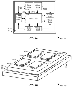
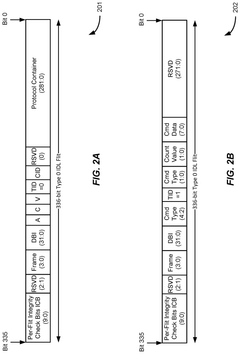
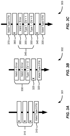
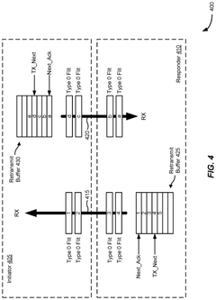
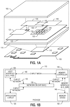
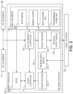
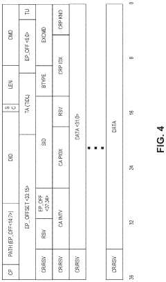
System-level techniques for error correction in chip-to-chip interfaces
PatentPendingUS20250030500A1
Innovation
- A retry-based error correction mechanism is implemented for chip-to-chip interfaces, which includes encoding data Flits to transmit control Flits, reducing the need for extra control signals, and utilizing Type-0 and Type-1 Flits for data and control messages respectively, with a retransmission mode triggered by error detection.
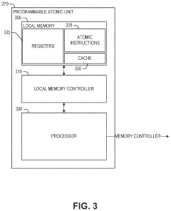
Method of executing programmable atomic unit resources within a multi-process system
PatentActiveUS12020062B2
Innovation
- A method is disclosed that involves determining a unique identifier for a programmable atomic transaction within a process, using a mapping table to generate a system-wide identifier, and issuing requests to a memory controller to perform the transaction, allowing for efficient execution and response handling through a programmable atomic unit.
Chiplet Ecosystem Development
The development of the chiplet ecosystem is a critical aspect of the evolving semiconductor industry, driven by the need for more efficient and scalable chip designs. This ecosystem encompasses a wide range of stakeholders, including chip designers, manufacturers, packaging companies, and tool providers, all working together to advance chiplet technology.
At the core of the chiplet ecosystem are the standardization efforts that enable interoperability between different chiplet designs. Organizations such as the Open Compute Project (OCP) and JEDEC have been instrumental in developing standards like Universal Chiplet Interconnect Express (UCIe), which provides a common framework for chiplet-to-chiplet communication. These standards are crucial for fostering innovation and competition within the ecosystem.
Foundries play a pivotal role in the chiplet ecosystem by providing advanced manufacturing processes for chiplets. Companies like TSMC, Samsung, and Intel are investing heavily in technologies such as advanced packaging and 3D integration, which are essential for realizing the full potential of chiplet architectures. These investments are driving the development of new manufacturing capabilities and processes specifically tailored for chiplet production.
The ecosystem also includes a growing number of chiplet IP providers, who offer pre-designed and validated chiplet components that can be integrated into larger systems. This modular approach allows for greater flexibility and faster time-to-market for complex chip designs. Companies specializing in specific functionalities, such as high-speed SerDes or memory interfaces, are emerging as key players in this space.
Design and verification tools are another crucial component of the chiplet ecosystem. EDA companies are developing specialized software to address the unique challenges of chiplet-based designs, including multi-die integration, thermal management, and signal integrity across chiplet interfaces. These tools are essential for enabling designers to effectively leverage chiplet technology in their products.
As the ecosystem matures, we are seeing increased collaboration between different players. For example, packaging companies are working closely with foundries and chip designers to develop advanced packaging solutions that can accommodate multiple chiplets in a single package. This collaboration is driving innovations in areas such as silicon interposers, through-silicon vias (TSVs), and advanced substrate technologies.
The chiplet ecosystem is also fostering new business models and supply chain dynamics. The ability to mix and match chiplets from different vendors is creating opportunities for specialized chiplet suppliers and enabling more flexible and resilient supply chains. This shift is particularly significant in the context of global semiconductor shortages and geopolitical tensions affecting the industry.
Chiplet Standardization Efforts
Chiplet standardization efforts have become increasingly crucial in the semiconductor industry as the adoption of chiplet architecture gains momentum. These initiatives aim to establish common protocols, interfaces, and design methodologies to facilitate interoperability and integration of chiplets from different vendors. The development of industry-wide standards is essential for realizing the full potential of chiplet technology and enabling a more diverse and competitive ecosystem.
One of the most prominent standardization efforts is the Universal Chiplet Interconnect Express (UCIe) consortium, which includes major players such as Intel, AMD, Arm, and TSMC. UCIe focuses on creating a standardized die-to-die interconnect that allows chiplets from various manufacturers to communicate seamlessly. This standard encompasses physical layer specifications, protocol stack definitions, and software abstractions to ensure compatibility across different chiplet implementations.
Another significant initiative is the Open Compute Project's (OCP) Chiplet Design Exchange (CDX) working group. CDX aims to develop open standards for chiplet-based designs, including reference architectures, design methodologies, and verification processes. By promoting open collaboration, CDX seeks to accelerate innovation and reduce development costs in the chiplet ecosystem.
The CHIPS Alliance, a Linux Foundation project, is also contributing to chiplet standardization efforts. Their focus is on creating open-source tools and methodologies for chiplet-based system design, including standardized interfaces and verification frameworks. This initiative aims to lower the barriers to entry for smaller companies and research institutions in the chiplet market.
Standardization efforts extend beyond interconnects and design methodologies to include packaging technologies. The Joint Electron Device Engineering Council (JEDEC) has been working on standards for advanced packaging technologies that are crucial for chiplet integration, such as through-silicon vias (TSVs) and interposers.
These collaborative efforts are essential for addressing key challenges in chiplet adoption, such as ensuring thermal management, power delivery, and signal integrity across heterogeneous chiplet assemblies. By establishing common standards, the industry can reduce design complexity, improve time-to-market, and foster innovation in chiplet-based solutions.
As chiplet technology continues to evolve, these standardization efforts will play a pivotal role in shaping the future of semiconductor design and manufacturing. They will enable a more modular and flexible approach to chip design, potentially revolutionizing the way complex systems are built and optimized for various applications, from high-performance computing to edge devices and beyond.
Unlock deeper insights with Patsnap Eureka Quick Research — get a full tech report to explore trends and direct your research. Try now!
Generate Your Research Report Instantly with AI Agent
Supercharge your innovation with Patsnap Eureka AI Agent Platform!