Chiplet Configuration: Pushing Boundaries in Digital Innovation
JUL 16, 20259 MIN READ
Generate Your Research Report Instantly with AI Agent
Patsnap Eureka helps you evaluate technical feasibility & market potential.
Chiplet Technology Evolution and Objectives
Chiplet technology has emerged as a revolutionary approach in the semiconductor industry, offering a paradigm shift in chip design and manufacturing. The evolution of chiplets can be traced back to the early 2010s when traditional monolithic chip designs began to face significant challenges in terms of scalability, performance, and cost-effectiveness. As Moore's Law reached its physical limits, chiplets presented a viable solution to continue advancing computing power and efficiency.
The primary objective of chiplet technology is to overcome the limitations of monolithic chip designs by disaggregating complex system-on-chip (SoC) architectures into smaller, more manageable components. This approach allows for greater flexibility in design, improved yield, and the ability to mix and match different process nodes within a single package. By enabling the integration of heterogeneous dies, chiplets aim to optimize performance, power consumption, and cost across a wide range of applications.
Throughout its evolution, chiplet technology has seen several key milestones. The initial concept focused on breaking down large dies into smaller, more easily manufacturable pieces. This was followed by the development of advanced packaging technologies, such as 2.5D and 3D integration, which allowed for the efficient interconnection of multiple chiplets. More recently, the industry has witnessed the emergence of standardized interfaces and protocols, such as Universal Chiplet Interconnect Express (UCIe), aimed at facilitating interoperability between chiplets from different vendors.
The technological trajectory of chiplets is closely aligned with the broader trends in the semiconductor industry, including the push for more energy-efficient computing, the rise of artificial intelligence and machine learning workloads, and the increasing demand for customized solutions in various market segments. As the technology matures, the objectives have expanded to include not only performance improvements but also enhanced reliability, reduced time-to-market, and greater design reuse.
Looking ahead, the chiplet ecosystem is poised for further innovation. Key objectives include refining die-to-die communication protocols, improving thermal management in multi-chiplet packages, and developing more sophisticated design and simulation tools. Additionally, there is a growing focus on creating a more robust supply chain and ecosystem around chiplet technology, with efforts to standardize chiplet interfaces and establish a marketplace for chiplet intellectual property (IP).
In conclusion, the evolution of chiplet technology represents a significant shift in the semiconductor landscape, with objectives that align closely with the industry's need for continued innovation in the face of physical and economic constraints. As research and development in this field progress, chiplets are expected to play an increasingly crucial role in shaping the future of digital innovation across various computing domains.
Market Demand for Chiplet-based Solutions
The market demand for chiplet-based solutions has been experiencing significant growth in recent years, driven by the increasing complexity and performance requirements of modern computing systems. As traditional monolithic chip designs reach their physical and economic limits, chiplet technology offers a promising alternative that addresses these challenges while meeting the evolving needs of various industries.
In the data center and cloud computing sector, there is a strong demand for chiplet-based solutions that can deliver higher performance, improved energy efficiency, and greater scalability. Large tech companies and cloud service providers are actively seeking chiplet configurations that can handle the growing computational demands of artificial intelligence, machine learning, and big data analytics workloads. These organizations require solutions that can offer flexible compute resources, reduced power consumption, and optimized thermal management.
The telecommunications industry, particularly with the rollout of 5G networks, is another key driver of chiplet demand. Network infrastructure providers are looking for chiplet-based solutions that can support the high-bandwidth, low-latency requirements of 5G technology while maintaining cost-effectiveness and power efficiency. Chiplets offer the ability to integrate diverse functionalities, such as radio frequency (RF) components, baseband processing, and network acceleration, into a single package, making them ideal for next-generation telecom equipment.
In the automotive sector, the transition towards autonomous vehicles and advanced driver assistance systems (ADAS) is fueling the demand for chiplet-based solutions. Automotive manufacturers and suppliers are seeking high-performance, reliable, and cost-effective computing platforms that can handle the complex sensor fusion, real-time decision-making, and safety-critical operations required in modern vehicles. Chiplets provide the flexibility to integrate different types of processors, accelerators, and memory components to meet these diverse requirements.
The consumer electronics market is also showing increased interest in chiplet technology, particularly for high-end smartphones, tablets, and gaming devices. Manufacturers are looking to leverage chiplets to create more powerful and energy-efficient devices with enhanced graphics capabilities, AI processing, and improved battery life. The ability to mix and match different chiplets allows for greater product differentiation and faster time-to-market.
As the Internet of Things (IoT) continues to expand, there is a growing demand for chiplet-based solutions in edge computing applications. Industries such as manufacturing, healthcare, and smart cities require compact, low-power computing solutions that can process data locally while maintaining connectivity to cloud services. Chiplets offer the potential to create customized, application-specific devices that balance performance, power consumption, and cost for diverse IoT use cases.
The market demand for chiplet-based solutions is further amplified by the need for more sustainable and environmentally friendly computing technologies. As organizations focus on reducing their carbon footprint, chiplets present an opportunity to improve overall system efficiency and extend the lifespan of existing hardware through modular upgrades.
Chiplet Configuration Challenges
Chiplet configuration presents several significant challenges in the realm of digital innovation. One of the primary obstacles is the complexity of interconnect design. As chiplets are separate dies that need to communicate with each other, designing efficient and high-bandwidth interconnects becomes crucial. This involves optimizing data transfer rates, minimizing latency, and ensuring signal integrity across different chiplets.
Another major challenge lies in thermal management. With multiple chiplets packed closely together, heat dissipation becomes a critical concern. Designers must develop innovative cooling solutions to prevent thermal throttling and maintain optimal performance. This may involve advanced packaging techniques, such as the use of thermal interface materials or integrated liquid cooling systems.
Power distribution and management across multiple chiplets also pose significant challenges. Ensuring uniform power delivery to each chiplet while managing voltage drops and current fluctuations requires sophisticated power delivery network designs. Moreover, implementing effective power gating and dynamic voltage and frequency scaling (DVFS) techniques across multiple chiplets adds another layer of complexity.
The integration of heterogeneous chiplets presents its own set of challenges. Combining chiplets manufactured using different process nodes or from different vendors introduces compatibility issues. These may include differences in I/O standards, power requirements, and timing characteristics. Overcoming these challenges requires careful system-level design and the development of standardized interfaces.
Testing and validation of chiplet-based systems are also more complex compared to monolithic designs. Each chiplet needs to be tested individually, and then the entire system must be validated as a whole. This requires advanced testing methodologies and equipment capable of handling multi-die configurations.
Yield management in chiplet production presents another challenge. While chiplets can potentially improve overall yield by allowing the use of smaller, higher-yield dies, managing the yield of the entire system becomes more complex. This includes considerations for known-good-die (KGD) testing and strategies for dealing with defective chiplets in the final assembly.
Lastly, the challenge of cost-effective manufacturing and assembly of chiplet-based systems cannot be overlooked. Developing economical processes for high-volume production, including advanced packaging technologies like 2.5D and 3D integration, is crucial for the widespread adoption of chiplet technology. This involves optimizing assembly processes, reducing material costs, and improving overall manufacturing yields.
Current Chiplet Configuration Approaches
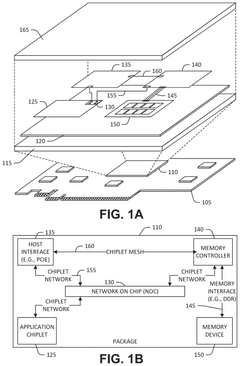
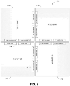
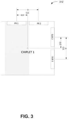
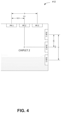
01 Chiplet interconnection and communication
This aspect focuses on the methods and systems for interconnecting multiple chiplets within a package. It includes techniques for high-speed data transfer between chiplets, optimizing communication protocols, and managing signal integrity across chiplet boundaries. These approaches aim to enhance overall system performance and efficiency in multi-chiplet configurations.- Chiplet interconnection and communication: This aspect focuses on the methods and systems for interconnecting multiple chiplets within a package. It includes techniques for high-speed data transfer between chiplets, optimizing signal integrity, and managing power distribution across chiplet boundaries. The designs aim to minimize latency and maximize bandwidth while maintaining thermal efficiency.
- Chiplet placement and orientation: This category covers strategies for optimal placement and orientation of chiplets within a package. It includes methods for determining the most efficient arrangement of chiplets to minimize signal path lengths, reduce power consumption, and improve overall system performance. Considerations for thermal management and manufacturing constraints are also addressed.
- Chiplet interface standardization: This point addresses the development and implementation of standardized interfaces for chiplets. It includes efforts to create common protocols and physical interfaces that allow chiplets from different manufacturers to be easily integrated. The goal is to promote interoperability and flexibility in chiplet-based system design.
- Chiplet power management and distribution: This aspect focuses on techniques for efficient power management and distribution across chiplet boundaries. It includes methods for dynamic power allocation, voltage regulation, and power gating to optimize energy consumption in multi-chiplet systems. Strategies for managing heat dissipation and thermal constraints are also considered.
- Chiplet testing and fault tolerance: This category covers methods for testing individual chiplets and ensuring fault tolerance in multi-chiplet systems. It includes techniques for pre- and post-assembly testing, error detection and correction across chiplet boundaries, and strategies for maintaining system functionality in the event of chiplet failures.
02 Thermal management and power distribution
This category addresses the challenges of heat dissipation and power delivery in chiplet-based designs. It covers innovative cooling solutions, power distribution networks, and thermal interface materials specifically tailored for multi-chiplet packages. These technologies are crucial for maintaining optimal performance and reliability in densely packed chiplet configurations.Expand Specific Solutions03 Chiplet integration and packaging technologies
This area encompasses advanced packaging techniques for integrating multiple chiplets into a single package. It includes 2.5D and 3D integration methods, interposer technologies, and novel substrate designs that enable efficient chiplet-to-chiplet and chiplet-to-package connections. These innovations aim to maximize performance while minimizing form factor in chiplet-based systems.Expand Specific Solutions04 Chiplet design and architecture optimization
This category focuses on optimizing the design and architecture of individual chiplets and their interactions within a multi-chiplet system. It includes methodologies for partitioning functionality across chiplets, standardizing chiplet interfaces, and developing modular chiplet architectures. These approaches aim to improve scalability, reusability, and overall system performance in chiplet-based designs.Expand Specific Solutions05 Testing and yield improvement for chiplet configurations
This aspect addresses the challenges of testing and improving yield in chiplet-based systems. It includes innovative test methodologies for individual chiplets and assembled multi-chiplet packages, as well as techniques for defect isolation and yield enhancement. These technologies are essential for ensuring the reliability and cost-effectiveness of chiplet-based products in high-volume manufacturing scenarios.Expand Specific Solutions
Key Players in Chiplet Industry
The research on Chiplet Configuration is currently in an early growth stage, with the market showing significant potential for expansion. The global chiplet market is projected to grow rapidly, driven by increasing demand for high-performance computing and AI applications. While the technology is still evolving, major players like Intel, AMD, and TSMC are making substantial investments in chiplet-based architectures. Companies such as Micron Technology, Qualcomm, and Samsung Electronics are also actively developing chiplet solutions, indicating a competitive landscape with diverse approaches. The technology's maturity varies across different applications, with some areas more advanced than others. As the industry progresses, we can expect increased collaboration and standardization efforts to overcome integration challenges and drive wider adoption of chiplet-based designs.
Intel Corp.
Technical Solution: Intel's Chiplet Configuration research focuses on their Foveros 3D packaging technology. This approach allows for stacking multiple chiplets vertically, enabling higher performance and lower power consumption. Intel's Meteor Lake processors utilize this technology, combining compute, graphics, and AI tiles[1]. The company has also developed the Advanced Interface Bus (AIB) for high-bandwidth, low-latency communication between chiplets[2]. Intel's research extends to their EMIB (Embedded Multi-die Interconnect Bridge) technology, which provides high-density interconnects between chiplets in a 2.5D configuration[3]. These innovations allow for more flexible and scalable chip designs, potentially reducing costs and improving yields in semiconductor manufacturing.
Strengths: Advanced 3D stacking capabilities, proprietary interconnect technologies, and established manufacturing processes. Weaknesses: Potential challenges in thermal management for 3D stacked designs and reliance on in-house technologies that may limit collaboration.
QUALCOMM, Inc.
Technical Solution: Qualcomm's Chiplet Configuration research centers on their heterogeneous integration approach for mobile and edge computing devices. Their technology focuses on integrating diverse chiplets, such as CPUs, GPUs, and AI accelerators, using advanced packaging techniques. Qualcomm has developed a proprietary die-to-die interconnect technology that enables high-bandwidth, low-latency communication between chiplets[4]. This approach allows for more efficient power management and performance optimization in space-constrained devices. Qualcomm's research also explores the use of chiplets in 5G modems, enabling more flexible and scalable designs for different market segments[5]. The company is investigating the potential of chiplets in automotive applications, aiming to create more adaptable and upgradable systems for advanced driver-assistance systems (ADAS) and autonomous driving[6].
Strengths: Expertise in mobile and edge computing, advanced die-to-die interconnect technology, and strong presence in 5G and automotive markets. Weaknesses: Potential challenges in scaling chiplet designs for high-performance computing applications and competition from integrated SoC solutions.
Core Innovations in Chiplet Integration
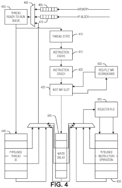
Variable pipeline length in a barrel-multithreaded processor
PatentActiveUS11847464B2
Innovation
- Implementing a variable pipeline length in processors to allow instructions to complete and writeback early, and using a scoreboard to detect and manage register writeback conflicts, ensuring efficient thread rescheduling and minimizing idle cycles.
Edge interface placements to enable chiplet rotation into multi-chiplet cluster
PatentPendingUS20240332257A1
Innovation
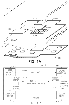
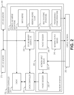
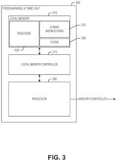
- The implementation of a chiplet architecture that uses a network-on-chip (NOC) with a chiplet protocol interface (CPI) to facilitate high-speed, flexible inter-chiplet communication, combined with a tightly packed matrix arrangement of chiplets and I/O micro-bumps for close-coupled interconnects, allowing for proper alignment and minimal footprint.
Standardization Efforts in Chiplet Technology
Standardization efforts in chiplet technology have become increasingly crucial as the industry moves towards more modular and heterogeneous chip designs. These efforts aim to establish common interfaces, protocols, and design methodologies that enable seamless integration of chiplets from different vendors. The development of industry-wide standards is essential for fostering innovation, reducing costs, and accelerating time-to-market for chiplet-based products.
One of the most prominent standardization initiatives is the Universal Chiplet Interconnect Express (UCIe) consortium. Launched in 2022, UCIe brings together major players in the semiconductor industry to define a universal interconnect standard for chiplets. The UCIe specification covers both the physical layer and the protocol layer, ensuring interoperability between chiplets from different manufacturers. This standard is designed to support a wide range of applications, from high-performance computing to mobile devices.
Another significant standardization effort is the Open Compute Project's (OCP) Chiplet Design Exchange (CDX) initiative. CDX focuses on creating an open ecosystem for chiplet-based designs, including standardized design methodologies, packaging technologies, and testing procedures. By promoting open standards, CDX aims to reduce barriers to entry for smaller companies and accelerate innovation in the chiplet space.
The CHIPS Alliance, an open-source hardware organization, is also contributing to chiplet standardization efforts. Their work includes developing open-source tools and methodologies for chiplet design and integration, as well as promoting interoperability between different chiplet technologies. The alliance's efforts are particularly focused on enabling more efficient and cost-effective chip design processes.
In addition to these industry-wide initiatives, several companies are developing their own chiplet standards and ecosystems. For example, AMD's Infinity Fabric and Intel's Advanced Interface Bus (AIB) are proprietary interconnect technologies that enable chiplet-based designs within their respective ecosystems. While these proprietary standards can offer optimized performance for specific applications, they may limit interoperability with chiplets from other vendors.
Standardization efforts in chiplet technology face several challenges, including balancing performance requirements with interoperability, addressing intellectual property concerns, and ensuring backward compatibility with existing chip designs. However, the potential benefits of standardization, such as reduced development costs, increased design flexibility, and accelerated innovation, are driving the industry towards greater collaboration and consensus-building in this area.
Economic Impact of Chiplet Adoption
The adoption of chiplet technology is poised to have a profound economic impact across the semiconductor industry and beyond. As traditional monolithic chip designs reach their physical and economic limits, chiplets offer a more flexible and cost-effective approach to semiconductor manufacturing. This shift is expected to drive significant changes in the industry's economic landscape.
One of the primary economic benefits of chiplet adoption is the potential for cost reduction in chip production. By allowing manufacturers to mix and match different functional blocks, chiplets enable the creation of customized solutions without the need for entirely new chip designs. This modular approach can lead to substantial savings in research and development costs, as well as reduced time-to-market for new products.
Furthermore, chiplet technology is likely to democratize access to advanced semiconductor capabilities. Smaller companies and startups, which may have previously been priced out of cutting-edge chip development, can now leverage chiplet designs to create innovative products without the massive capital investments required for traditional chip fabrication. This could lead to increased competition and innovation in the semiconductor market.
The chiplet approach also has the potential to improve supply chain resilience. By diversifying the production of different functional blocks across multiple manufacturers, companies can reduce their reliance on a single supplier and mitigate the risks associated with geopolitical tensions or natural disasters that could disrupt production.
From a macroeconomic perspective, the widespread adoption of chiplets could contribute to economic growth by enabling advancements in various technology sectors. As chiplets facilitate the development of more powerful and efficient computing systems, they are likely to accelerate progress in fields such as artificial intelligence, 5G communications, and the Internet of Things. This, in turn, could drive productivity gains across multiple industries.
However, the transition to chiplet-based designs may also present economic challenges. Established semiconductor companies may need to adapt their business models and invest in new manufacturing processes to remain competitive. This could lead to short-term disruptions in the industry as companies realign their strategies and resources.
In conclusion, the economic impact of chiplet adoption is expected to be far-reaching, potentially reshaping the semiconductor industry's competitive landscape, driving innovation, and enabling new technological capabilities across various sectors of the global economy.
Unlock deeper insights with Patsnap Eureka Quick Research — get a full tech report to explore trends and direct your research. Try now!
Generate Your Research Report Instantly with AI Agent
Supercharge your innovation with Patsnap Eureka AI Agent Platform!