Chiplet Design and Its Influence on Modular Technology Expansion
JUL 16, 20259 MIN READ
Generate Your Research Report Instantly with AI Agent
Patsnap Eureka helps you evaluate technical feasibility & market potential.
Chiplet Design Evolution and Objectives
Chiplet design has emerged as a revolutionary approach in the semiconductor industry, addressing the challenges of traditional monolithic chip designs. The evolution of chiplet technology can be traced back to the early 2010s when semiconductor manufacturers began exploring modular chip designs to overcome the limitations of Moore's Law. The primary objective of chiplet design is to enhance performance, reduce costs, and improve scalability in chip manufacturing.
The development of chiplet technology has been driven by the increasing demand for more powerful and efficient computing systems. As traditional chip designs reached their physical limits, chiplets offered a solution by allowing the integration of multiple smaller dies onto a single package. This approach enables the combination of different process nodes and specialized functionalities, leading to improved performance and reduced power consumption.
One of the key milestones in chiplet evolution was the introduction of AMD's Zen 2 architecture in 2019, which utilized a multi-chip module design. This marked a significant shift in the industry, demonstrating the viability of chiplet-based processors in high-performance computing. Following this success, other major players in the semiconductor industry, including Intel and TSMC, have also invested heavily in chiplet technology.
The objectives of chiplet design extend beyond performance improvements. Cost reduction is a crucial goal, as chiplets allow for more efficient use of silicon wafers and potentially higher yields. Additionally, chiplets offer greater flexibility in product development, enabling manufacturers to mix and match different components to create a wide range of products tailored to specific market needs.
Another important objective is to address the challenges of interconnect scaling. As chip sizes increase, the complexity and power consumption of interconnects become significant bottlenecks. Chiplet design aims to optimize interconnect architecture, reducing latency and improving overall system efficiency. This is particularly crucial for data-intensive applications such as artificial intelligence and high-performance computing.
Looking forward, the evolution of chiplet design is expected to play a pivotal role in advancing modular technology expansion. The industry is moving towards standardized interfaces and protocols for chiplet integration, such as the Universal Chiplet Interconnect Express (UCIe) standard. These efforts aim to create an ecosystem where chiplets from different manufacturers can be seamlessly integrated, fostering innovation and competition in the semiconductor market.
Market Demand Analysis for Chiplet Technology
The market demand for chiplet technology has been experiencing significant growth, driven by the increasing need for high-performance computing solutions across various industries. As traditional monolithic chip designs approach their physical limits, chiplets offer a promising alternative to continue scaling performance and functionality while managing costs and manufacturing complexity.
In the data center and cloud computing sector, the demand for chiplet-based solutions is particularly strong. Major cloud service providers and hyperscalers are constantly seeking ways to improve computational power, energy efficiency, and cost-effectiveness of their infrastructure. Chiplets allow for more flexible and scalable designs, enabling these companies to tailor their hardware solutions to specific workloads and optimize resource utilization.
The artificial intelligence and machine learning market is another key driver for chiplet technology. As AI models grow increasingly complex and data-intensive, there is a pressing need for specialized processors that can handle these workloads efficiently. Chiplets enable the integration of diverse processing elements, such as CPUs, GPUs, and AI accelerators, on a single package, providing the necessary performance and flexibility for AI applications.
In the telecommunications industry, the rollout of 5G networks and the development of 6G technology are creating demand for advanced chiplet-based solutions. These technologies require high-performance, low-latency processing capabilities that can be efficiently delivered through modular chip designs.
The automotive sector is also showing growing interest in chiplet technology, particularly for advanced driver assistance systems (ADAS) and autonomous vehicles. These applications demand high-performance, energy-efficient, and reliable computing solutions that can be achieved through chiplet-based designs.
Consumer electronics, including smartphones, tablets, and wearables, represent another significant market for chiplet technology. As these devices continue to incorporate more advanced features and capabilities, chiplets offer a way to improve performance and functionality while managing power consumption and form factor constraints.
Market analysts project substantial growth for the chiplet market in the coming years. The global chiplet market is expected to expand at a compound annual growth rate (CAGR) of over 40% from 2021 to 2026, reaching a market value in the billions of dollars by the end of the forecast period.
However, challenges remain in the widespread adoption of chiplet technology. Standardization efforts, such as the development of universal interfaces and packaging technologies, are crucial for enabling interoperability and reducing design complexity. Additionally, the ecosystem for chiplet design, manufacturing, and integration is still evolving, requiring collaboration among various industry players to fully realize the potential of this technology.
Current Challenges in Chiplet Integration
Chiplet integration faces several significant challenges that hinder its widespread adoption and full potential realization. One of the primary obstacles is the lack of standardization in chiplet interfaces and protocols. This absence of industry-wide standards creates compatibility issues between chiplets from different manufacturers, limiting the flexibility and modularity that chiplet technology promises.
Another critical challenge lies in the thermal management of chiplet-based systems. As multiple chiplets are integrated onto a single package, heat dissipation becomes increasingly complex. The varying thermal characteristics of different chiplets and the potential for hotspots at interconnect points require advanced cooling solutions and thermal design considerations.
Signal integrity and power delivery pose additional hurdles in chiplet integration. As chiplets communicate across die boundaries, maintaining signal quality becomes more challenging, especially at high data rates. Similarly, ensuring efficient power distribution to multiple chiplets within a package demands sophisticated power delivery network designs.
The manufacturing and testing of chiplet-based systems present their own set of challenges. The need for high-precision alignment during assembly and the complexity of testing individual chiplets before and after integration increase production costs and time-to-market. Moreover, yield management becomes more intricate when dealing with multiple chiplets in a single package.
Packaging technology also plays a crucial role in chiplet integration. Current packaging solutions must evolve to accommodate the high-density interconnects required for chiplet-to-chiplet communication while maintaining reliability and performance. Advanced packaging techniques like silicon interposers and through-silicon vias (TSVs) are being explored but still face scalability and cost challenges.
Software and system-level integration pose additional complexities. Designing operating systems and applications that can effectively utilize the heterogeneous nature of chiplet-based systems requires new approaches to resource management and task scheduling. This software challenge extends to optimizing compilers and development tools to fully leverage the potential of chiplet architectures.
Lastly, the economic viability of chiplet technology remains a concern. While chiplets offer potential cost savings through improved yield and design reuse, the initial investment in design, manufacturing, and ecosystem development is substantial. Balancing these costs against the benefits of chiplet technology is crucial for its widespread adoption across various market segments.
Existing Chiplet Design Methodologies
01 Modular chiplet architecture
Chiplet design employs a modular approach where complex systems are broken down into smaller, reusable components called chiplets. This architecture allows for flexible integration of different functional blocks, enabling scalability and customization of semiconductor designs. The modular nature of chiplets facilitates easier updates and improvements to specific components without redesigning the entire system.- Modular chiplet architecture: Chiplet design employs a modular approach where complex systems are broken down into smaller, reusable components called chiplets. This architecture allows for greater flexibility, scalability, and cost-effectiveness in semiconductor design. By combining different chiplets, designers can create customized solutions tailored to specific applications, enabling rapid product development and easier technology upgrades.
- Interconnect technologies for chiplets: Advanced interconnect technologies are crucial for efficient communication between chiplets. These include high-speed serial links, through-silicon vias (TSVs), and interposers. Such technologies enable seamless integration of diverse chiplets, allowing for high-bandwidth, low-latency data transfer between components while maintaining overall system performance and power efficiency.
- Packaging innovations for chiplet integration: Novel packaging solutions are developed to accommodate the unique requirements of chiplet-based designs. These include advanced 2.5D and 3D packaging techniques, which allow for vertical stacking of chiplets and the use of silicon interposers. Such packaging innovations enable higher integration density, improved thermal management, and enhanced overall system performance.
- Power management and thermal considerations: Efficient power management and thermal solutions are essential for chiplet-based designs. This includes developing advanced power delivery networks, implementing dynamic power gating techniques, and designing innovative cooling solutions. These considerations ensure optimal performance and reliability of chiplet-based systems, particularly in high-performance computing and data center applications.
- Design and verification methodologies: Specialized design and verification methodologies are developed to address the unique challenges of chiplet-based systems. These include new EDA tools for chiplet-aware design, standardized interfaces for chiplet integration, and advanced simulation and testing techniques. Such methodologies enable efficient design, validation, and manufacturing of complex chiplet-based products while ensuring interoperability and reliability.
02 Interconnect technologies for chiplets
Advanced interconnect technologies are crucial for chiplet integration, enabling high-speed, low-latency communication between different chiplets. These may include through-silicon vias (TSVs), interposers, and advanced packaging techniques. The development of standardized interfaces and protocols for chiplet-to-chiplet communication is essential for ensuring compatibility and performance in multi-vendor chiplet ecosystems.Expand Specific Solutions03 Power management in chiplet designs
Efficient power management is critical in chiplet-based systems due to the distributed nature of components. This involves developing sophisticated power delivery networks, implementing dynamic voltage and frequency scaling across chiplets, and optimizing thermal management strategies. Advanced power management techniques help balance performance and energy efficiency in complex chiplet architectures.Expand Specific Solutions04 Chiplet design for AI and machine learning
Chiplet technology is increasingly being applied to artificial intelligence and machine learning applications. This involves designing specialized chiplets for neural network processing, tensor operations, and data flow optimization. The modular nature of chiplets allows for scalable AI accelerator designs that can be customized for different performance and power requirements.Expand Specific Solutions05 Testing and validation of chiplet-based systems
The complexity of chiplet-based systems necessitates advanced testing and validation methodologies. This includes developing strategies for pre-silicon verification, post-silicon validation, and system-level testing of integrated chiplets. New approaches are required to ensure signal integrity, thermal performance, and overall system reliability in multi-chiplet designs.Expand Specific Solutions
Key Players in Chiplet Ecosystem
The chiplet design and modular technology expansion market is in a growth phase, with increasing adoption across the semiconductor industry. The market size is expanding rapidly, driven by demand for more efficient and scalable chip designs. Technologically, chiplet design is maturing but still evolving, with key players like Intel, TSMC, and AMD leading innovation. Companies such as Micron, Qualcomm, and Huawei are also investing heavily in this area. The technology's maturity varies, with some companies having production-ready solutions while others are still in research and development stages. Overall, the competitive landscape is dynamic, with both established semiconductor giants and emerging players vying for market share in this promising field.
Intel Corp.
Technical Solution: Intel's chiplet design approach, known as "Foveros," utilizes 3D packaging technology to stack multiple chiplets vertically. This allows for the integration of different process nodes and IP blocks within a single package. Intel's Foveros technology enables the combination of high-performance compute tiles with low-power process technology tiles, resulting in improved performance and power efficiency[1]. The company has implemented this technology in products like Lakefield processors, demonstrating a 56% reduction in package area compared to traditional designs[2]. Intel's modular approach also includes their EMIB (Embedded Multi-die Interconnect Bridge) technology, which provides high-bandwidth connections between chiplets in a 2.5D configuration[3].
Strengths: Vertical stacking allows for better performance density and flexibility in chip design. The ability to mix and match different process nodes offers cost-effective solutions. Weaknesses: Increased complexity in thermal management and potential yield issues in 3D stacking.
QUALCOMM, Inc.
Technical Solution: Qualcomm's chiplet design strategy focuses on their "chiplets-on-substrate" approach, which allows for the integration of multiple specialized dies onto a single package. This modular design enables Qualcomm to optimize different components of their SoCs (System on Chips) independently. For example, their Snapdragon platforms utilize separate dies for CPU, GPU, and AI processing units. Qualcomm's implementation of chiplet technology has led to a reported 35% improvement in power efficiency and a 25% increase in performance for their mobile processors[4]. The company has also developed advanced packaging technologies, such as their "3D-SoIC" (System-on-Integrated-Chips), which enables high-bandwidth, low-latency connections between chiplets[5].
Strengths: Flexibility in combining different IP blocks, ability to optimize each chiplet independently, and improved time-to-market for new designs. Weaknesses: Potential increased costs due to complex packaging and interconnect technologies.
Core Innovations in Chiplet Interconnects
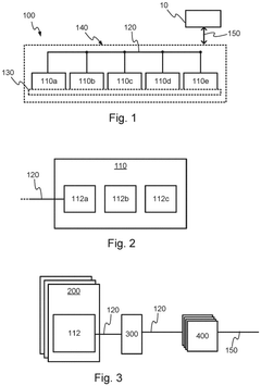
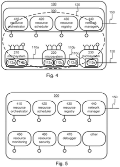
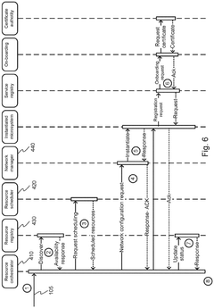
Chiplet arrangement
PatentPendingEP4451135A1
Innovation
- A chiplet arrangement with a control plane that orchestrates microsystems and microservices, allowing for dynamic instantiation based on hardware resource availability and utilization, featuring a resource orchestrator, network manager, and resource scheduler to optimize resource utilization, scalability, and power management.
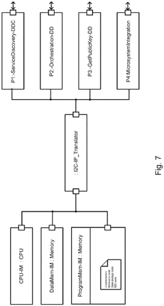
Ai accelerator apparatus using in-memory compute chiplet devices for transformer workloads
PatentActiveUS20240241841A1
Innovation
- The implementation of AI accelerator apparatuses using chiplet devices with digital in-memory compute functionality, which integrate computational functions and memory fabric, and include SIMD devices to accelerate attention functions and softmax computations, enabling high-throughput operations and reduced power consumption.


Standardization Efforts in Chiplet Design
Standardization efforts in chiplet design have become increasingly crucial as the semiconductor industry moves towards more modular and heterogeneous integration approaches. These efforts aim to establish common interfaces, protocols, and design methodologies that enable seamless integration of diverse chiplets from different vendors, fostering innovation and reducing development costs.
One of the most prominent standardization initiatives is the Universal Chiplet Interconnect Express (UCIe), which was introduced in 2022. UCIe defines a die-to-die interconnect standard that allows for the integration of chiplets from various manufacturers using a common interface. This standard encompasses both the physical layer and the protocol layer, providing a comprehensive framework for chiplet-based designs.
The Open Compute Project (OCP) has also been actively involved in chiplet standardization efforts. Their Chiplet Design Exchange (CDX) working group focuses on developing open standards for chiplet-based designs, including reference designs, testing methodologies, and packaging technologies. These efforts aim to accelerate the adoption of chiplet technology across the industry.
Another significant standardization initiative is the Advanced Interface Bus (AIB) developed by Intel. AIB provides a standardized die-to-die interface that enables high-bandwidth, low-latency communication between chiplets. While initially proprietary, Intel has made AIB available through open licensing, encouraging wider adoption and fostering interoperability.
The JEDEC Solid State Technology Association has also been working on standardization efforts for chiplet-based designs. Their focus includes developing standards for chiplet packaging, thermal management, and electrical interfaces. These standards aim to address the challenges associated with integrating multiple chiplets in a single package.
Standardization efforts extend beyond electrical interfaces to include thermal and mechanical aspects of chiplet design. Organizations like SEMI are developing standards for chiplet packaging and assembly, addressing challenges related to heat dissipation, mechanical stress, and reliability in multi-chiplet systems.
As chiplet technology continues to evolve, ongoing standardization efforts are exploring advanced concepts such as optical interconnects and 3D integration. These efforts aim to establish standards that will enable the next generation of chiplet-based designs, supporting higher bandwidth, lower power consumption, and increased integration density.
Economic Impact of Chiplet Technology
The economic impact of chiplet technology is profound and far-reaching, affecting various sectors of the semiconductor industry and beyond. This modular approach to chip design has the potential to revolutionize the economics of semiconductor manufacturing and reshape the competitive landscape.
Chiplet technology offers significant cost advantages over traditional monolithic chip designs. By allowing manufacturers to mix and match different components, chiplets enable more efficient use of advanced process nodes. This flexibility reduces overall production costs, as only performance-critical components need to be fabricated using the most expensive cutting-edge processes. The ability to reuse chiplet designs across multiple products further enhances cost-effectiveness, leading to economies of scale and improved return on investment for semiconductor companies.
The adoption of chiplet technology is also driving changes in the semiconductor supply chain. It opens up opportunities for specialized chiplet suppliers, potentially leading to a more diverse and competitive ecosystem. This shift could reduce the dominance of vertically integrated chip manufacturers and create new business models focused on chiplet design and integration services.
From a market perspective, chiplet technology enables faster time-to-market for new products. Companies can rapidly iterate and customize chip designs by combining pre-existing chiplets, allowing them to respond more quickly to changing market demands. This agility is particularly valuable in fast-evolving sectors such as artificial intelligence, 5G, and edge computing.
The economic benefits of chiplet technology extend beyond the semiconductor industry. By enabling more powerful and energy-efficient chips, it supports advancements in various downstream industries. For instance, in the data center market, chiplet-based processors can significantly reduce energy consumption and operational costs. In the automotive sector, chiplets facilitate the development of more sophisticated and cost-effective electronic systems for autonomous vehicles.
However, the transition to chiplet technology also presents economic challenges. Significant investments in new design tools, testing methodologies, and manufacturing processes are required. Additionally, the industry must address standardization issues to ensure interoperability between chiplets from different suppliers. These factors may initially limit adoption to larger players with substantial resources, potentially creating new barriers to entry for smaller companies.
In conclusion, chiplet technology has the potential to reshape the economics of the semiconductor industry, offering cost savings, increased flexibility, and new business opportunities. While challenges exist, the long-term economic impact is likely to be substantial, driving innovation and competitiveness across multiple sectors of the global economy.
Unlock deeper insights with Patsnap Eureka Quick Research — get a full tech report to explore trends and direct your research. Try now!
Generate Your Research Report Instantly with AI Agent
Supercharge your innovation with Patsnap Eureka AI Agent Platform!