Chiplet Integration in Adaptive Control Interface Design
JUL 16, 20259 MIN READ
Generate Your Research Report Instantly with AI Agent
Patsnap Eureka helps you evaluate technical feasibility & market potential.
Chiplet Integration Background and Objectives
Chiplet integration has emerged as a revolutionary approach in the semiconductor industry, addressing the challenges of traditional monolithic chip design. This technology enables the disaggregation of complex system-on-chip (SoC) designs into smaller, more manageable chiplets, which can be manufactured separately and then integrated onto a single package. The evolution of chiplet technology can be traced back to the early 2000s, with significant advancements occurring in the past decade.
The primary objective of chiplet integration in adaptive control interface design is to enhance system flexibility, improve performance, and reduce costs. By leveraging chiplets, designers can mix and match different process nodes, intellectual property (IP) blocks, and functionalities to create highly customized and optimized solutions. This approach allows for the integration of heterogeneous components, each manufactured using the most suitable process technology, resulting in improved overall system performance and efficiency.
As Moore's Law faces increasing challenges, chiplet integration offers a promising alternative to continue scaling and improving semiconductor devices. The technology aims to overcome the limitations of monolithic designs, such as yield issues, thermal constraints, and rising manufacturing costs associated with advanced process nodes. By enabling the use of mature process nodes for less critical components while reserving cutting-edge processes for performance-critical elements, chiplet integration provides a more cost-effective and scalable solution.
The adaptive control interface design plays a crucial role in chiplet integration, as it facilitates seamless communication and coordination between different chiplets within a package. The objectives of this research include developing standardized interfaces, optimizing data transfer protocols, and implementing efficient power management strategies across multiple chiplets. Additionally, the adaptive control interface must address challenges related to thermal management, signal integrity, and system-level optimization to ensure optimal performance and reliability of the integrated chiplet-based system.
Another key goal of chiplet integration research is to establish industry-wide standards and ecosystems that promote interoperability and reduce design complexity. This includes developing common protocols, packaging technologies, and testing methodologies that enable chiplets from different vendors to work together seamlessly. By fostering collaboration and standardization, the industry aims to accelerate innovation, reduce time-to-market, and create new opportunities for specialized chip designs across various applications, including high-performance computing, artificial intelligence, and edge computing.
Market Analysis for Adaptive Control Interfaces
The market for adaptive control interfaces integrated with chiplet technology is experiencing significant growth and transformation. This convergence of technologies is driven by the increasing demand for more flexible, efficient, and powerful computing solutions across various industries. The adaptive control interface market, which encompasses a wide range of applications from industrial automation to consumer electronics, is projected to expand rapidly in the coming years.
One of the key factors driving market demand is the need for more sophisticated control systems in complex environments. Industries such as aerospace, automotive, and manufacturing are increasingly relying on adaptive control interfaces to manage intricate processes and optimize performance. The integration of chiplet technology into these interfaces offers enhanced processing capabilities, improved energy efficiency, and greater scalability, making them particularly attractive for high-performance applications.
In the consumer electronics sector, the demand for adaptive control interfaces is being fueled by the growing popularity of smart home devices and wearable technology. These interfaces, when combined with chiplet-based designs, can offer more responsive and personalized user experiences while maintaining compact form factors and extended battery life.
The healthcare industry is another significant market for adaptive control interfaces with chiplet integration. Medical devices and diagnostic equipment benefit from the increased processing power and adaptability offered by these technologies, enabling more accurate and real-time patient monitoring and treatment delivery.
Market analysis indicates that the Asia-Pacific region is expected to witness the highest growth rate in the adaptive control interface market. This is primarily due to the rapid industrialization, increasing adoption of automation technologies, and substantial investments in research and development in countries like China, Japan, and South Korea.
North America and Europe are also substantial markets, with a strong focus on innovation and early adoption of advanced technologies. The presence of major technology companies and research institutions in these regions is driving continuous advancements in adaptive control interfaces and chiplet integration.
The market is characterized by intense competition among key players, including both established semiconductor companies and emerging startups. This competitive landscape is fostering innovation and driving down costs, making adaptive control interfaces with chiplet integration more accessible to a broader range of applications and industries.
As the Internet of Things (IoT) and edge computing continue to evolve, the demand for adaptive control interfaces with integrated chiplet technology is expected to surge. These interfaces will play a crucial role in managing the vast amounts of data generated by IoT devices and enabling real-time decision-making at the edge.
Chiplet Technology: Current State and Challenges
Chiplet technology has emerged as a revolutionary approach in semiconductor design and manufacturing, offering a promising solution to the challenges faced by traditional monolithic chip designs. The current state of chiplet technology is characterized by significant advancements in integration techniques, interconnect technologies, and packaging solutions. However, it also faces several challenges that need to be addressed for wider adoption and implementation.
One of the primary advantages of chiplet technology is its ability to overcome the limitations of Moore's Law by enabling the integration of multiple smaller dies onto a single package. This approach allows for better yield management, cost reduction, and improved performance scaling. Currently, leading semiconductor companies are actively developing and implementing chiplet-based designs in their high-performance computing and data center products.
The state-of-the-art in chiplet technology involves advanced packaging techniques such as 2.5D and 3D integration. These methods utilize interposers or through-silicon vias (TSVs) to connect multiple chiplets, enabling high-bandwidth and low-latency communication between different functional blocks. The industry has also made significant progress in developing standardized interfaces for chiplet-to-chiplet communication, such as the Advanced Interface Bus (AIB) and Universal Chiplet Interconnect Express (UCIe).
Despite these advancements, chiplet technology faces several challenges. One of the most significant hurdles is the need for improved thermal management solutions. As chiplets are densely packed and stacked, heat dissipation becomes a critical issue that can impact performance and reliability. Researchers are exploring novel cooling techniques, including microfluidic cooling and advanced thermal interface materials, to address this challenge.
Another major challenge lies in the design and verification of chiplet-based systems. The complexity of integrating multiple chiplets with different functionalities and potentially from different vendors requires sophisticated design tools and methodologies. Ensuring signal integrity, power distribution, and timing closure across chiplet boundaries presents significant technical difficulties that need to be overcome.
Furthermore, the industry is grappling with the challenge of standardization. While efforts like UCIe are underway, there is still a need for broader adoption of common interfaces and protocols to enable true mix-and-match capabilities across different chiplet vendors. This standardization is crucial for creating a robust ecosystem and realizing the full potential of chiplet technology.
In the context of adaptive control interface design, chiplet integration presents both opportunities and challenges. The modular nature of chiplets allows for more flexible and customizable control interfaces, potentially enabling adaptive systems that can reconfigure themselves based on changing requirements or environmental conditions. However, implementing such adaptive interfaces across chiplet boundaries requires overcoming significant design and integration challenges, particularly in terms of maintaining low-latency communication and ensuring seamless coordination between different chiplets.
Existing Chiplet Integration Solutions for Control Interfaces
01 Adaptive control interfaces for chiplet integration
Adaptive control interfaces are developed to manage the integration of chiplets in multi-chip systems. These interfaces dynamically adjust communication protocols, power management, and data transfer rates between chiplets to optimize overall system performance and efficiency. The adaptive nature allows for seamless integration of heterogeneous chiplets with varying capabilities and requirements.- Adaptive control interfaces for chiplet integration: Adaptive control interfaces are developed to manage the integration of chiplets in multi-chip systems. These interfaces dynamically adjust communication protocols, power management, and data transfer rates between chiplets to optimize overall system performance and efficiency. The adaptive nature allows for real-time adjustments based on workload, thermal conditions, and power constraints.
- Inter-chiplet communication optimization: Techniques for optimizing communication between chiplets are implemented, focusing on reducing latency and improving bandwidth. This includes the development of high-speed interconnects, advanced signaling methods, and intelligent routing algorithms. The optimization process considers factors such as distance between chiplets, data priority, and system architecture to enhance overall performance.
- Power management and thermal control in chiplet systems: Advanced power management and thermal control mechanisms are integrated into chiplet systems. These systems dynamically allocate power resources among chiplets, implement fine-grained power gating, and utilize adaptive cooling techniques. The goal is to maintain optimal performance while minimizing power consumption and preventing thermal issues in densely packed chiplet configurations.
- Reconfigurable interconnect fabrics for chiplet integration: Reconfigurable interconnect fabrics are designed to facilitate flexible chiplet integration. These fabrics allow for dynamic adjustment of connections between chiplets, enabling system-level optimization and fault tolerance. The reconfigurability supports various chiplet arrangements and can adapt to different application requirements or compensate for potential chiplet failures.
- AI-driven chiplet integration and management: Artificial intelligence techniques are employed to enhance chiplet integration and management. AI algorithms are used for predictive maintenance, workload distribution, and dynamic system optimization. These intelligent systems can learn from operational patterns, anticipate potential issues, and make proactive adjustments to maintain peak performance and reliability in complex chiplet-based architectures.
02 Inter-chiplet communication optimization
Techniques for optimizing inter-chiplet communication are implemented to enhance data transfer efficiency and reduce latency. This includes adaptive routing algorithms, dynamic bandwidth allocation, and intelligent buffer management. The optimization process considers factors such as chiplet proximity, data priority, and system workload to ensure optimal utilization of available resources.Expand Specific Solutions03 Power management and thermal control in chiplet systems
Advanced power management and thermal control mechanisms are integrated into chiplet systems. These mechanisms use adaptive algorithms to monitor and adjust power consumption and heat distribution across multiple chiplets. The system can dynamically allocate power budgets, adjust clock frequencies, and manage thermal hotspots to maintain optimal performance while ensuring system stability and longevity.Expand Specific Solutions04 Reconfigurable interconnects for flexible chiplet integration
Reconfigurable interconnect architectures are developed to support flexible chiplet integration. These interconnects can adapt their topology, bandwidth, and protocol to accommodate different chiplet configurations and requirements. This flexibility allows for easier integration of new chiplets, improved fault tolerance, and the ability to optimize system performance based on specific application needs.Expand Specific Solutions05 AI-driven chiplet integration and optimization
Artificial intelligence techniques are employed to enhance chiplet integration and system optimization. Machine learning algorithms are used to predict system behavior, optimize chiplet placement, and dynamically adjust control parameters. This AI-driven approach enables continuous improvement in system performance, energy efficiency, and reliability through adaptive learning and real-time optimization.Expand Specific Solutions
Key Players in Chiplet and Adaptive Control Industries
The research on Chiplet Integration in Adaptive Control Interface Design is in an emerging phase, with significant potential for growth. The market is expanding rapidly due to increasing demand for advanced semiconductor solutions in various industries. While the technology is still evolving, several key players are making substantial progress. Companies like Intel, Xilinx, and Micron Technology are at the forefront, leveraging their expertise in semiconductor design and manufacturing. Other notable contributors include Huawei Technologies and Samsung Electronics, who are investing heavily in this area. The competitive landscape is dynamic, with both established semiconductor giants and innovative startups vying for market share in this promising field.
Micron Technology, Inc.
Technical Solution: Micron's approach to chiplet integration in adaptive control interface design centers around their Hybrid Memory Cube (HMC) technology and advanced memory solutions. They focus on developing high-bandwidth, low-latency memory interfaces that can efficiently support chiplet-based architectures[13]. Micron's adaptive control interface design incorporates their Open Memory Interface (OMI) technology, which provides a flexible and scalable memory subsystem for chiplet integration. Their research includes developing intelligent memory controllers that can dynamically adjust memory access patterns and power states based on workload demands, enhancing overall system efficiency[14]. Micron also explores the use of through-silicon vias (TSVs) and advanced packaging techniques to enable closer integration of memory chiplets with processing elements, reducing latency and improving power efficiency in adaptive control systems[15].
Strengths: Expertise in high-performance memory solutions, flexible memory interfaces, and advanced packaging technologies. Weaknesses: Limited focus on non-memory aspects of chiplet integration and potential challenges in system-level optimization.
Xilinx, Inc.
Technical Solution: Xilinx's approach to chiplet integration in adaptive control interface design leverages their Adaptive Compute Acceleration Platform (ACAP) architecture. This platform combines programmable logic, embedded processing, and AI engines in a chiplet-based design[7]. For adaptive control, Xilinx implements a Network-on-Chip (NoC) that dynamically manages communication between chiplets, adjusting bandwidth and routing based on real-time demands. Their Versal ACAP series incorporates an AI Engine that can be used to optimize chiplet interconnect configurations and workload distribution[8]. Xilinx also utilizes their Stacked Silicon Interconnect (SSI) technology to enable high-bandwidth, low-latency connections between chiplets, supporting adaptive control mechanisms across the entire system[9].
Strengths: Highly flexible and reconfigurable architecture, integrated AI capabilities for optimization, and advanced interconnect technologies. Weaknesses: Potential learning curve for developers and higher power consumption compared to ASIC solutions.
Core Innovations in Chiplet-based Adaptive Control Design
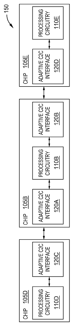
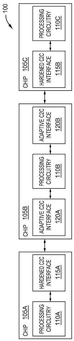
Adaptive chip-to-chip interface protocol architecture
PatentWO2023146588A1
Innovation
- An adaptive chip-to-chip interface that supports multiple protocols, allowing configuration during boot time to match the protocol of connected chips, enabling communication between chips with hardened and adaptive interfaces.
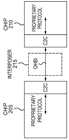
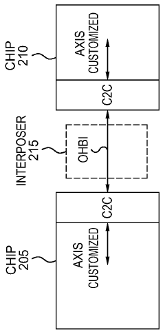
Edge interface placements to enable chiplet rotation into multi-chiplet cluster
PatentPendingUS20240332257A1
Innovation
- The implementation of a chiplet architecture that uses a network-on-chip (NOC) with a chiplet protocol interface (CPI) to facilitate high-speed, flexible inter-chiplet communication, combined with a tightly packed matrix arrangement of chiplets and I/O micro-bumps for close-coupled interconnects, allowing for proper alignment and minimal footprint.
Thermal Management in Chiplet-based Control Interfaces
Thermal management is a critical aspect of chiplet-based control interfaces, as the integration of multiple chiplets in a single package can lead to significant heat generation and distribution challenges. The compact nature of chiplet designs often results in higher power densities, making efficient heat dissipation crucial for maintaining optimal performance and reliability.
One of the primary thermal management strategies in chiplet-based control interfaces involves the use of advanced packaging technologies. These include the implementation of through-silicon vias (TSVs) and interposers, which not only facilitate electrical connections between chiplets but also aid in heat distribution. TSVs, in particular, can be designed to serve as thermal conduits, allowing for more efficient heat transfer from the active layers to the package substrate and heat spreader.
The design of the package substrate itself plays a vital role in thermal management. Materials with high thermal conductivity, such as copper-based substrates or advanced ceramic materials, are often employed to enhance heat spreading. Additionally, the incorporation of embedded heat pipes or vapor chambers within the substrate can significantly improve heat distribution across the package, reducing hotspots and ensuring more uniform temperature profiles.
Active cooling solutions are frequently integrated into chiplet-based control interfaces to address the increased thermal demands. These may include miniaturized liquid cooling systems, where coolant is circulated through microchannels etched directly into the silicon or integrated into the package. Such solutions offer superior cooling performance compared to traditional air cooling methods, particularly for high-power applications.
Thermal interface materials (TIMs) are another critical component in the thermal management strategy. Advanced TIMs with high thermal conductivity and low thermal resistance are used to improve heat transfer between the chiplets, substrate, and heat spreader. Emerging technologies in this area include the use of phase-change materials and graphene-based composites, which offer enhanced thermal performance and reliability.
Dynamic thermal management techniques are increasingly being implemented in chiplet-based designs. These involve real-time monitoring of temperature distributions across the package and adaptive control of power consumption and clock frequencies. By dynamically adjusting the performance of individual chiplets based on thermal conditions, these systems can optimize overall system performance while maintaining safe operating temperatures.
Standardization Efforts in Chiplet Integration
Standardization efforts in chiplet integration have become increasingly crucial as the semiconductor industry moves towards more modular and heterogeneous chip designs. These efforts aim to establish common protocols, interfaces, and design methodologies to enable seamless integration of diverse chiplets from different vendors. The DARPA CHIPS (Common Heterogeneous Integration and IP Reuse Strategies) program has been instrumental in driving these standardization initiatives, fostering collaboration among industry leaders and research institutions.
One of the key standardization efforts is the development of the Advanced Interface Bus (AIB) specification. AIB provides a standardized die-to-die interface that allows for high-bandwidth, low-latency communication between chiplets. This specification has gained significant traction in the industry, with major players like Intel and TSMC adopting and promoting its use. The AIB standard enables designers to mix and match chiplets from different sources, promoting innovation and reducing development costs.
Another important standardization initiative is the Bunch of Wires (BoW) interface, developed by the Open Compute Project (OCP). BoW offers a simpler, more cost-effective alternative to AIB for applications that require lower bandwidth. This standard is particularly suitable for chiplets that don't demand the highest performance levels, making it an attractive option for a wide range of applications.
The Universal Chiplet Interconnect Express (UCIe) consortium, formed by industry giants such as Intel, AMD, Arm, and TSMC, is working on developing a comprehensive standard for chiplet integration. UCIe aims to create an open ecosystem for chiplet-based designs, covering aspects such as physical layer specifications, protocol stack, and software interfaces. This standardization effort is expected to significantly accelerate the adoption of chiplet technology across the industry.
In the realm of packaging technologies, the Joint Electron Device Engineering Council (JEDEC) has been actively developing standards for advanced packaging solutions. These standards address critical aspects of chiplet integration, including thermal management, signal integrity, and power delivery. JEDEC's efforts ensure that chiplet-based designs can meet the stringent requirements of modern electronic systems.
The IEEE has also contributed to chiplet standardization through its P2851 standard for 3D stacked die interfaces. This standard focuses on the vertical integration of chiplets, addressing challenges related to through-silicon vias (TSVs) and interposer technologies. By providing guidelines for 3D integration, IEEE P2851 complements other standardization efforts and expands the possibilities for chiplet-based system designs.
Unlock deeper insights with Patsnap Eureka Quick Research — get a full tech report to explore trends and direct your research. Try now!
Generate Your Research Report Instantly with AI Agent
Supercharge your innovation with Patsnap Eureka AI Agent Platform!