

Chiplet Options for Next-Level High-Definition Graphics Processing
JUL 16, 20259 MIN READ
Generate Your Research Report Instantly with AI Agent
PatSnap Eureka helps you evaluate technical feasibility & market potential.
Chiplet Technology Evolution and Objectives
Chiplet technology has emerged as a revolutionary approach in the semiconductor industry, particularly in the realm of high-performance computing and graphics processing. The evolution of chiplets can be traced back to the early 2010s when traditional monolithic chip designs began to face significant challenges in terms of scalability, yield, and cost-effectiveness. As Moore's Law slowed down, chiplets offered a promising solution to continue advancing semiconductor performance and capabilities.
The primary objective of chiplet technology in the context of high-definition graphics processing is to overcome the limitations of traditional monolithic GPU designs. By disaggregating complex GPU architectures into smaller, more manageable chiplets, manufacturers aim to achieve higher performance, improved yield, and greater flexibility in design and manufacturing processes. This approach allows for the integration of heterogeneous components, each optimized for specific functions, resulting in more efficient and powerful graphics processing units.
The evolution of chiplet technology in graphics processing has been marked by several key milestones. Initially, the focus was on developing effective interconnect technologies to enable high-bandwidth, low-latency communication between chiplets. This led to the development of advanced packaging technologies such as 2.5D and 3D integration, which have become crucial for chiplet-based GPU designs.
As the technology matured, major GPU manufacturers began incorporating chiplet designs into their product roadmaps. AMD's RDNA 3 architecture, for instance, represents a significant step forward in chiplet-based GPU design, demonstrating the viability and potential of this approach for high-performance graphics processing.
The current objectives of chiplet technology in graphics processing are multifaceted. Firstly, there is a strong focus on improving energy efficiency, as chiplets allow for more granular power management and optimization of individual components. Secondly, manufacturers are aiming to push the boundaries of performance by leveraging the scalability of chiplet designs to create more powerful GPUs with higher core counts and memory bandwidth.
Another key objective is to enhance manufacturing flexibility and cost-effectiveness. Chiplet technology allows for the mix-and-match of different process nodes, enabling manufacturers to optimize performance and cost by using cutting-edge processes only where necessary. This approach also improves yield rates, as smaller chiplets are less prone to defects compared to large monolithic dies.
Looking ahead, the future objectives of chiplet technology in graphics processing include further miniaturization and integration of components, exploration of new interconnect technologies to reduce latency and increase bandwidth between chiplets, and the development of more sophisticated power management techniques to maximize performance within thermal constraints.
Market Demand for Advanced Graphics Processing
The demand for advanced graphics processing has been steadily increasing across various sectors, driven by the growing need for high-definition visual experiences in gaming, virtual reality, artificial intelligence, and professional visualization applications. The market for next-level graphics processing units (GPUs) is experiencing significant growth, with a particular focus on chiplet-based solutions that offer improved performance, power efficiency, and scalability.
In the gaming industry, the push for higher resolution displays, faster frame rates, and more realistic graphics has created a substantial demand for more powerful GPUs. As 4K gaming becomes mainstream and 8K gaming emerges on the horizon, the need for advanced graphics processing capabilities continues to escalate. This trend is further amplified by the rising popularity of ray tracing and other computationally intensive rendering techniques that require substantial processing power.
The virtual and augmented reality (VR/AR) market is another key driver for advanced graphics processing. As VR/AR technologies mature and find applications beyond gaming, such as in training simulations, architectural visualization, and remote collaboration, the demand for high-fidelity, low-latency graphics processing grows. These applications require GPUs capable of rendering complex 3D environments in real-time while maintaining high frame rates to prevent motion sickness and ensure user comfort.
In the professional visualization sector, industries such as film production, scientific research, and product design rely heavily on advanced graphics processing for tasks like 3D modeling, rendering, and simulation. The increasing complexity of these tasks, coupled with the need for faster turnaround times, drives the demand for more powerful and efficient GPUs.
The artificial intelligence and machine learning fields also contribute significantly to the market demand for advanced graphics processing. GPUs have become essential for training and running complex neural networks, with applications ranging from autonomous vehicles to natural language processing. As AI models grow in size and complexity, the need for more powerful and specialized graphics processing solutions intensifies.
The data center and cloud computing markets represent another substantial source of demand for advanced graphics processing. With the growth of cloud gaming services, remote workstations, and GPU-accelerated computing in data centers, there is a rising need for scalable, high-performance graphics processing solutions that can be efficiently deployed in large-scale environments.
As the demand for advanced graphics processing continues to grow across these diverse sectors, chiplet-based solutions emerge as a promising approach to address the challenges of performance scaling, power efficiency, and manufacturing costs. The modular nature of chiplets allows for more flexible and scalable GPU designs, potentially enabling manufacturers to meet the varied demands of different market segments more effectively.
Current Challenges in Chiplet-based GPU Design
The integration of chiplet technology in GPU design presents several significant challenges that need to be addressed for successful implementation. One of the primary obstacles is the interconnect bandwidth between chiplets. As GPUs require high-speed data transfer between different components, ensuring sufficient bandwidth and low latency in inter-chiplet communication is crucial. Current interconnect technologies struggle to meet the demanding requirements of high-performance graphics processing, potentially limiting the overall system performance.
Another challenge lies in thermal management and power distribution across multiple chiplets. GPUs are known for their high power consumption and heat generation. When distributing the processing across multiple chiplets, maintaining efficient cooling and power delivery becomes more complex. Ensuring uniform heat dissipation and preventing thermal hotspots across the chiplet array is essential for maintaining stable performance and longevity of the GPU.
The design and optimization of the chiplet floor plan pose additional challenges. Determining the optimal arrangement of chiplets, considering factors such as data flow, thermal distribution, and signal integrity, requires sophisticated planning and simulation. The increased complexity of chiplet-based designs may lead to longer development cycles and higher costs, which need to be balanced against the potential benefits of improved yield and scalability.
Manufacturing and testing processes also present hurdles in chiplet-based GPU design. Ensuring consistent quality and performance across multiple chiplets from potentially different manufacturing processes or even different foundries can be challenging. Additionally, developing effective testing methodologies for individual chiplets and the integrated system is crucial for maintaining high quality standards and yield rates.
Lastly, software and driver development for chiplet-based GPUs introduces new complexities. Optimizing software to efficiently utilize the distributed nature of chiplet-based architectures, managing memory access across chiplets, and ensuring seamless integration with existing graphics APIs and software ecosystems are critical challenges that need to be addressed for widespread adoption of chiplet-based GPU designs.
Existing Chiplet Solutions for Graphics Processing
01 Chiplet-based GPU architecture
Graphics processing units (GPUs) are being designed using chiplet architecture, where multiple smaller dies are interconnected to form a larger, more powerful GPU. This approach allows for improved scalability, better yield, and potentially lower manufacturing costs compared to monolithic designs.- Chiplet-based GPU architecture: Graphics processing units (GPUs) are being designed using chiplet technology, where multiple smaller dies are combined to form a larger, more powerful GPU. This approach allows for improved scalability, better yield, and potentially lower manufacturing costs compared to monolithic designs.
- Inter-chiplet communication for graphics processing: Efficient communication between chiplets is crucial for graphics processing performance. Advanced interconnect technologies and protocols are being developed to ensure high-bandwidth, low-latency data transfer between different chiplets in a GPU system.
- Memory integration in chiplet-based GPUs: Chiplet-based GPU designs are incorporating various memory architectures, including high-bandwidth memory (HBM) stacks or dedicated memory chiplets. These approaches aim to optimize memory bandwidth and capacity for graphics processing tasks.
- Power management in multi-chiplet GPUs: Efficient power management techniques are being developed for chiplet-based GPUs to optimize performance and energy consumption. These include dynamic power gating, voltage scaling, and intelligent workload distribution across chiplets.
- Rendering and compute optimization for chiplet GPUs: Novel algorithms and techniques are being developed to optimize rendering and compute tasks for chiplet-based GPU architectures. These include workload balancing, task scheduling, and parallel processing strategies tailored for multi-chiplet systems.
02 Inter-chiplet communication for graphics processing
Efficient communication between chiplets is crucial for graphics processing performance. Advanced interconnect technologies and protocols are being developed to ensure high-bandwidth, low-latency data transfer between different chiplets in a GPU system.Expand Specific Solutions03 Memory integration in chiplet-based GPUs
Chiplet-based GPU designs are incorporating various memory architectures, including high-bandwidth memory (HBM) stacks and on-chip caches, to optimize data access and reduce latency in graphics processing tasks.Expand Specific Solutions04 Power management in multi-chiplet GPUs
Efficient power management techniques are being developed for chiplet-based GPUs to optimize performance and energy consumption across multiple dies. This includes dynamic voltage and frequency scaling, as well as intelligent workload distribution among chiplets.Expand Specific Solutions05 Rendering and compute optimization for chiplet GPUs
Novel algorithms and techniques are being developed to optimize rendering and compute tasks for chiplet-based GPU architectures. These include load balancing, task scheduling, and parallel processing strategies tailored for multi-die configurations.Expand Specific Solutions
Key Players in Chiplet and GPU Industries
The research on chiplet options for next-level high-definition graphics processing is in a dynamic phase, with the market showing significant growth potential. The technology is advancing rapidly, driven by increasing demand for high-performance computing and AI applications. Key players like Intel, AMD, NVIDIA, and Qualcomm are at the forefront, investing heavily in chiplet technology. These companies are leveraging their expertise in semiconductor design and manufacturing to develop innovative solutions. The market is characterized by intense competition and collaboration, with companies like Samsung, BOE, and ZTE also making strides. As the technology matures, we can expect to see more specialized applications and increased adoption across various industries.
Intel Corp.
Technical Solution: Intel's approach to chiplet-based graphics processing focuses on their Xe architecture, which utilizes a modular design philosophy. Their Ponte Vecchio GPU, designed for high-performance computing and AI workloads, incorporates multiple chiplets or "tiles" manufactured using different process nodes[4]. This heterogeneous integration allows Intel to optimize each component for its specific function. The Xe Link interconnect technology enables high-bandwidth, low-latency communication between chiplets, crucial for graphics processing tasks. Intel's implementation also includes advanced packaging technologies like Foveros 3D and EMIB (Embedded Multi-die Interconnect Bridge) to stack and connect chiplets efficiently[5]. For graphics-specific applications, Intel is developing specialized compute and cache tiles to enhance ray tracing and AI-assisted rendering capabilities[6].
Strengths: Flexible and scalable architecture, advanced packaging technologies, and ability to optimize different components separately. Weaknesses: Relatively new to high-end GPU market, still catching up in terms of software ecosystem and driver optimization.
QUALCOMM, Inc.
Technical Solution: Qualcomm's approach to chiplet technology in graphics processing is primarily focused on mobile and embedded systems. Their Snapdragon series, while not traditionally considered in the high-end desktop GPU space, has been incorporating advanced packaging techniques to improve graphics performance in mobile devices. Qualcomm's strategy involves integrating their Adreno GPUs with other system components using a System-in-Package (SiP) approach[9]. This allows for tighter integration between the GPU, CPU, and other specialized processors. For next-level high-definition graphics, Qualcomm is exploring the use of advanced packaging technologies to create more powerful and efficient mobile GPUs. Their research includes developing high-bandwidth, low-power interconnects suitable for chiplet-based designs in mobile form factors[10]. Additionally, Qualcomm is investing in AI-enhanced graphics processing, which could potentially be implemented in a chiplet-based architecture to offload specific tasks from the main GPU core.
Strengths: Expertise in mobile GPU design, power-efficient architectures, and integration with 5G and AI technologies. Weaknesses: Limited experience in high-end desktop GPU market, focus primarily on mobile and embedded systems.
Core Innovations in Chiplet Interconnect Technologies
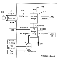
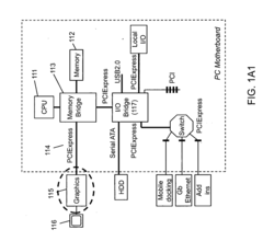
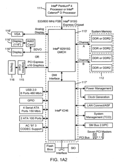
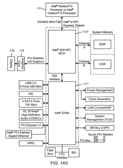
Graphics subsytem for integation in a PC-based computing system and providing multiple GPU-driven pipeline cores supporting multiple modes of parallelization dynamically controlled while running a graphics application
PatentInactiveUS20080129745A1
Innovation
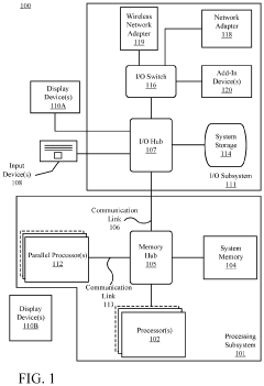
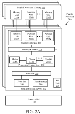
- A multi-pipeline system-on-chip (MP-SOC) architecture with multiple graphic cores integrated on a single silicon chip, enabling flexible parallelization schemes and adaptive support for different modes of parallelism within both geometry and pixel processing subsystems, bypassing the converge bottleneck and addressing the limitations of single GPU systems and multi-GPU systems.
Out-of-order pixel shading and rasterization
PatentActiveUS20220414967A1
Innovation
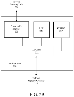
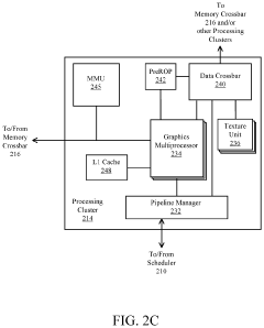
- A GPU architecture with a parallel processing unit that incorporates a scheduler, processing clusters, and memory crossbar to distribute workloads efficiently across multiple processing clusters, enabling SIMT architecture for parallel processing of graphics and machine-learning operations.
Thermal Management Strategies for Chiplet GPUs
Thermal management is a critical aspect of chiplet-based GPU design, particularly as the industry moves towards higher performance and more compact form factors. The integration of multiple chiplets in a single package introduces unique thermal challenges that must be addressed to ensure optimal performance and reliability.
One of the primary thermal management strategies for chiplet GPUs involves advanced packaging technologies. These include the use of high-performance thermal interface materials (TIMs) between the chiplets and the heat spreader, as well as between the heat spreader and the cooling solution. Materials such as indium-based solders or liquid metal TIMs offer superior thermal conductivity compared to traditional thermal pastes, enabling more efficient heat dissipation from the chiplets.
Another key approach is the implementation of sophisticated heat spreading techniques. This may involve the use of vapor chambers or heat pipes integrated directly into the GPU package. These solutions help to distribute heat more evenly across the entire surface area of the cooling solution, preventing localized hotspots that can occur due to the concentrated heat generation of individual chiplets.
Active cooling solutions play a crucial role in chiplet GPU thermal management. Advanced fan designs, such as those incorporating vapor chamber technology or utilizing multiple smaller fans for targeted cooling, can significantly enhance heat dissipation. Additionally, liquid cooling solutions are becoming increasingly popular for high-performance chiplet GPUs, offering superior thermal performance and the potential for quieter operation.
Power management and thermal-aware task scheduling are software-based strategies that complement hardware solutions. By dynamically adjusting clock speeds and voltages of individual chiplets based on their thermal conditions, the overall thermal envelope of the GPU can be optimized. This approach allows for maintaining high performance while preventing thermal throttling.
Emerging technologies such as on-chip microfluidic cooling channels are being explored for future chiplet GPU designs. These innovative solutions promise to provide more direct and efficient cooling to individual chiplets, potentially enabling even higher performance and density in next-generation graphics processors.
As chiplet GPU designs continue to evolve, thermal management strategies will need to adapt accordingly. The industry is likely to see a combination of advanced materials, innovative packaging techniques, and intelligent thermal management algorithms working in concert to address the thermal challenges posed by increasingly powerful and compact chiplet-based graphics processors.
Standardization Efforts in Chiplet Technologies
Standardization efforts in chiplet technologies have become increasingly crucial as the industry moves towards more modular and heterogeneous chip designs. These efforts aim to establish common interfaces, protocols, and design methodologies that enable seamless integration of diverse chiplets from different vendors. The JEDEC Solid State Technology Association has been at the forefront of these standardization initiatives, developing specifications such as the Universal Chiplet Interconnect Express (UCIe).
UCIe represents a significant milestone in chiplet standardization, providing a unified interconnect standard that supports both die-to-die and package-to-package communication. This standard encompasses physical layer, protocol layer, and software stack specifications, facilitating interoperability between chiplets from various manufacturers. The adoption of UCIe by major industry players, including Intel, AMD, Arm, and TSMC, underscores its potential to become the de facto standard for chiplet integration.
Another important standardization effort is the Open Compute Project's Bunch of Wires (BoW) interface. BoW aims to provide a simple, cost-effective die-to-die interconnect solution that can be implemented across different process nodes. This standard is particularly relevant for chiplet-based designs that prioritize cost-efficiency and flexibility over maximum performance.
The Advanced Interface Bus (AIB) consortium, led by Intel, has also been working on standardizing chiplet interfaces. AIB focuses on high-bandwidth, low-latency connections between chiplets, making it suitable for performance-critical applications such as high-definition graphics processing. The latest version, AIB 2.0, offers improved power efficiency and higher data rates compared to its predecessor.
In the realm of 3D chip stacking, the 3D-IC Alliance has been driving standardization efforts for through-silicon via (TSV) technology. This initiative aims to establish common design rules, testing methodologies, and manufacturing processes for 3D-stacked chiplets, which are particularly relevant for next-generation graphics processing units that require high-density integration.
The CHIPS Alliance, an open-source hardware initiative, has been working on standardizing chiplet design and verification tools. Their efforts include developing open-source IP blocks and design methodologies that can accelerate the adoption of chiplet-based architectures across the industry.
As these standardization efforts continue to evolve, they are expected to play a crucial role in enabling the widespread adoption of chiplet technologies for next-level high-definition graphics processing. By establishing common interfaces and design practices, these standards will facilitate the creation of more modular, scalable, and cost-effective GPU architectures that can meet the ever-increasing demands of advanced graphics applications.
Unlock deeper insights with PatSnap Eureka Quick Research — get a full tech report to explore trends and direct your research. Try now!
Generate Your Research Report Instantly with AI Agent
Supercharge your innovation with PatSnap Eureka AI Agent Platform!