

Resistive RAM Developments and Semiconductor Patent Trends
OCT 9, 20259 MIN READ
Generate Your Research Report Instantly with AI Agent
PatSnap Eureka helps you evaluate technical feasibility & market potential.
ReRAM Technology Evolution and Objectives
Resistive Random Access Memory (ReRAM) has emerged as a promising non-volatile memory technology over the past two decades, evolving from theoretical concepts to commercial products. The technology's development can be traced back to the early 2000s when researchers observed resistive switching phenomena in various metal oxide materials. This discovery laid the foundation for what would become one of the most promising candidates for next-generation memory solutions.
The evolution of ReRAM technology has been characterized by significant improvements in material science, device architecture, and fabrication processes. Initially, simple metal-oxide-metal structures demonstrated basic switching capabilities but suffered from poor reliability and endurance. By the mid-2000s, researchers had begun exploring various oxide materials including HfOx, TaOx, and TiOx, which showed improved switching characteristics and compatibility with CMOS processes.
A critical milestone in ReRAM development occurred around 2010-2012 when several semiconductor companies demonstrated integrated ReRAM arrays with selectors, addressing the sneak path current issue that had previously limited array scaling. This period also saw the refinement of switching mechanisms, with clearer understanding of filamentary and interface-type switching behaviors that govern ReRAM operation.
The patent landscape reflects this technological progression, with early patents focusing on basic material compositions and simple device structures, while more recent intellectual property emphasizes integration schemes, reliability enhancement techniques, and novel applications beyond traditional memory storage.
Current objectives in ReRAM development are multifaceted, addressing both technical challenges and market positioning. From a technical perspective, key goals include improving endurance beyond 10^12 cycles, reducing operating voltages below 1V, enhancing retention at elevated temperatures, and achieving multi-bit storage capabilities through precise resistance state control. Scaling remains another critical objective, with efforts directed toward sub-10nm technology nodes to compete with established memory technologies.
From a market perspective, ReRAM aims to position itself in specific application niches where its unique characteristics provide advantages over competing technologies. These include embedded applications requiring low power consumption, neuromorphic computing systems leveraging ReRAM's analog behavior for in-memory computing, and edge AI devices benefiting from ReRAM's non-volatility and fast switching speeds.
The convergence of semiconductor manufacturing capabilities with innovative material engineering has accelerated ReRAM development in recent years. Industry collaborations between material suppliers, equipment manufacturers, and integrated device manufacturers have been instrumental in addressing fabrication challenges and establishing standardized evaluation methodologies, which are essential for technology maturation and market adoption.
Market Demand Analysis for Non-Volatile Memory
The non-volatile memory market has experienced significant growth over the past decade, driven primarily by the increasing demand for data storage solutions across various sectors. The global non-volatile memory market was valued at approximately $67 billion in 2022 and is projected to reach $110 billion by 2028, representing a compound annual growth rate (CAGR) of 8.6%. This growth trajectory is underpinned by the proliferation of data-intensive applications and the expanding digital ecosystem.
Consumer electronics continues to be the largest end-user segment for non-volatile memory, accounting for nearly 40% of the market share. The rapid adoption of smartphones, tablets, and other portable devices has fueled the demand for high-capacity, energy-efficient memory solutions. Additionally, the automotive sector has emerged as a significant growth driver, with advanced driver-assistance systems (ADAS) and in-vehicle infotainment systems requiring robust non-volatile memory components.
Enterprise storage systems represent another crucial market segment, particularly with the ongoing digital transformation initiatives across industries. The shift towards cloud computing and big data analytics has intensified the need for reliable, high-performance memory solutions capable of handling massive data volumes. Data centers worldwide are increasingly incorporating non-volatile memory technologies to enhance processing speeds and reduce power consumption.
The Internet of Things (IoT) ecosystem presents a substantial opportunity for non-volatile memory manufacturers. With billions of connected devices generating unprecedented amounts of data, the demand for edge computing capabilities has surged. Resistive RAM (ReRAM) and other emerging non-volatile memory technologies are well-positioned to address this demand due to their low power consumption and high endurance characteristics.
Geographically, Asia-Pacific dominates the non-volatile memory market, accounting for approximately 45% of global revenue. This regional prominence is attributed to the concentration of semiconductor manufacturing facilities and the robust electronics industry in countries like South Korea, Japan, Taiwan, and China. North America follows as the second-largest market, driven by technological innovation and substantial investments in data center infrastructure.
The market landscape is witnessing a gradual shift from traditional non-volatile memory technologies like NAND and NOR flash towards emerging alternatives such as ReRAM, MRAM, and PCM. This transition is motivated by the inherent limitations of conventional technologies in meeting the escalating performance requirements of modern applications. Industry analysts predict that these emerging technologies will capture approximately 15% of the non-volatile memory market by 2026, up from less than 5% in 2021.
ReRAM Technical Challenges and Global Development Status
ReRAM technology faces several significant technical challenges that have impacted its widespread adoption despite its promising characteristics. One of the primary obstacles is the variability in resistance states, which affects data reliability and retention. This inconsistency manifests as fluctuations in the high and low resistance states over time, potentially leading to data corruption or loss. The root cause lies in the complex physical mechanisms governing filament formation and dissolution within the oxide layer.
Another critical challenge is the endurance limitation of ReRAM cells. Current implementations typically achieve 10^6 to 10^8 write cycles, which falls short of the requirements for certain high-intensity memory applications. This limitation stems from gradual degradation of the switching material due to repeated ion migration and structural changes at the atomic level.
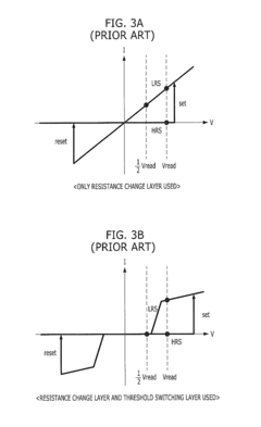
The sneak path current issue in crossbar array architectures represents a significant design challenge. Without proper isolation mechanisms, parasitic currents can flow through unselected cells, causing read errors and increased power consumption. Various selector devices have been proposed to address this issue, but each introduces additional complexity and manufacturing considerations.
From a global development perspective, ReRAM research and commercialization efforts are concentrated in several key regions. The United States leads in fundamental research, with institutions like Stanford University and companies such as Micron Technology and Intel making significant contributions. Japan maintains a strong position through companies like Panasonic and Fujitsu, which have demonstrated working prototypes with promising characteristics.
South Korea has emerged as a major player, with Samsung and SK Hynix investing heavily in ReRAM development as part of their memory portfolio diversification strategy. In Europe, research institutions in Germany and France are focusing on novel materials and integration schemes for ReRAM, while China has rapidly increased its patent filings and research output in recent years, particularly through companies like YMTC and academic institutions.
The global patent landscape reveals an accelerating trend in ReRAM-related intellectual property, with annual filings increasing by approximately 15% year-over-year since 2015. Material innovation patents dominate the field, followed by architecture and integration methods. This distribution reflects the industry's focus on overcoming the fundamental material challenges while simultaneously developing practical implementation approaches.
Despite these challenges, recent breakthroughs in hafnium oxide-based ReRAM and tantalum oxide systems have demonstrated improved reliability metrics, suggesting that technical solutions are gradually emerging to address the core limitations of this promising technology.
Another critical challenge is the endurance limitation of ReRAM cells. Current implementations typically achieve 10^6 to 10^8 write cycles, which falls short of the requirements for certain high-intensity memory applications. This limitation stems from gradual degradation of the switching material due to repeated ion migration and structural changes at the atomic level.
The sneak path current issue in crossbar array architectures represents a significant design challenge. Without proper isolation mechanisms, parasitic currents can flow through unselected cells, causing read errors and increased power consumption. Various selector devices have been proposed to address this issue, but each introduces additional complexity and manufacturing considerations.
From a global development perspective, ReRAM research and commercialization efforts are concentrated in several key regions. The United States leads in fundamental research, with institutions like Stanford University and companies such as Micron Technology and Intel making significant contributions. Japan maintains a strong position through companies like Panasonic and Fujitsu, which have demonstrated working prototypes with promising characteristics.
South Korea has emerged as a major player, with Samsung and SK Hynix investing heavily in ReRAM development as part of their memory portfolio diversification strategy. In Europe, research institutions in Germany and France are focusing on novel materials and integration schemes for ReRAM, while China has rapidly increased its patent filings and research output in recent years, particularly through companies like YMTC and academic institutions.
The global patent landscape reveals an accelerating trend in ReRAM-related intellectual property, with annual filings increasing by approximately 15% year-over-year since 2015. Material innovation patents dominate the field, followed by architecture and integration methods. This distribution reflects the industry's focus on overcoming the fundamental material challenges while simultaneously developing practical implementation approaches.
Despite these challenges, recent breakthroughs in hafnium oxide-based ReRAM and tantalum oxide systems have demonstrated improved reliability metrics, suggesting that technical solutions are gradually emerging to address the core limitations of this promising technology.
Current ReRAM Implementation Approaches
01 Resistive RAM device structures
Resistive RAM (RRAM) devices are constructed with specific structural configurations to optimize performance. These structures typically include a resistive switching layer sandwiched between two electrodes. Various materials can be used for the resistive layer, including metal oxides, chalcogenides, and perovskites. The electrode materials and their interfaces with the resistive layer play crucial roles in determining switching characteristics. Advanced structures may incorporate additional layers for improved stability, retention, and endurance.- Materials and structures for RRAM devices: Resistive Random Access Memory (RRAM) devices utilize specific materials and structures to enable resistive switching behavior. These typically include metal oxides like HfO2, TiO2, or Ta2O5 as the switching layer sandwiched between two electrodes. The structure may incorporate additional layers such as barrier layers or doping elements to enhance performance. The specific arrangement of these materials significantly impacts the device's switching characteristics, endurance, and retention properties.
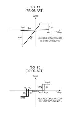
- Switching mechanisms and operation principles: RRAM operation is based on the formation and rupture of conductive filaments within the resistive switching layer. The switching mechanism involves the migration of oxygen vacancies or metal ions under an applied electric field, creating or breaking conductive paths. This results in reversible transitions between high-resistance (HRS) and low-resistance states (LRS). Different operation modes include unipolar switching, where the same voltage polarity is used for both SET and RESET operations, and bipolar switching, which requires opposite voltage polarities.
- Integration and fabrication techniques: Fabrication of RRAM devices involves specialized techniques to ensure proper formation of the resistive switching layer and electrode interfaces. These include atomic layer deposition (ALD), physical vapor deposition (PVD), and various etching processes. Integration challenges include ensuring compatibility with CMOS processes, minimizing cell-to-cell variability, and developing 3D stacking architectures to increase memory density. Advanced fabrication methods focus on controlling the microstructure and defect concentration in the switching layer.
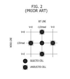
- Circuit design and array architecture: RRAM array architectures require specific circuit designs to address individual memory cells and manage the read/write operations. Common configurations include crossbar arrays, where memory cells are placed at the intersection of word and bit lines. Peripheral circuits include sense amplifiers for reading the resistance state, write drivers for programming operations, and address decoders. Advanced designs incorporate selector devices to mitigate sneak path currents in high-density arrays and implement multi-level cell capabilities for increased storage density.
- Performance enhancement and reliability improvement: Enhancing RRAM performance involves addressing key challenges such as endurance, retention, and switching variability. Techniques include interface engineering to control the formation of conductive filaments, doping the switching layer to modify its electrical properties, and optimizing the programming algorithms. Reliability improvements focus on reducing the variability of SET and RESET operations, minimizing read disturbance, and extending the device lifetime through stress-induced degradation mitigation. Advanced approaches include self-compliance mechanisms and multi-layer stacks to enhance stability.
02 Resistive switching mechanisms
The operation of resistive RAM relies on various switching mechanisms that enable transitions between high and low resistance states. These mechanisms include filamentary conduction, where conductive filaments form and rupture within the resistive layer, and interface-type switching, where resistance changes occur at the electrode-oxide interfaces. Other mechanisms involve vacancy migration, redox reactions, and phase changes in the switching material. Understanding these mechanisms is essential for designing reliable RRAM devices with consistent performance characteristics.Expand Specific Solutions03 Memory array architectures
Resistive RAM can be integrated into various memory array architectures to create high-density storage solutions. These architectures include crossbar arrays, where memory cells are positioned at the intersections of word and bit lines, and 3D stacked structures that maximize storage density. Advanced architectures incorporate selector devices to mitigate sneak path currents and improve read/write operations. The design of peripheral circuits for addressing, sensing, and programming also plays a critical role in overall memory performance.Expand Specific Solutions04 Fabrication methods and materials
The manufacturing of resistive RAM involves specialized fabrication techniques and material selections. Common approaches include atomic layer deposition, sputtering, and sol-gel methods for creating the resistive switching layer. Various materials are employed, such as HfOx, TaOx, TiOx for oxide-based RRAM, and GeSbTe for phase-change variants. Doping strategies can enhance switching characteristics and reliability. Integration with CMOS processes enables compatibility with existing semiconductor manufacturing infrastructure, facilitating commercial adoption.Expand Specific Solutions05 Performance optimization techniques
Various techniques are employed to optimize the performance of resistive RAM devices. These include pulse engineering, where the shape, amplitude, and duration of programming pulses are carefully controlled to improve switching reliability and reduce power consumption. Interface engineering modifies the electrode-oxide interfaces to enhance stability and reduce variability. Thermal management strategies prevent undesired thermal effects during operation. Additionally, error correction codes and adaptive programming algorithms can be implemented to improve data retention and endurance characteristics.Expand Specific Solutions
Key Industry Players and Patent Holders
The Resistive RAM (ReRAM) market is currently in a growth phase, with an estimated market size of $300-500 million and projected significant expansion as memory demands increase across IoT, AI, and edge computing applications. The technology has reached moderate maturity, with key players advancing commercial viability. Leading semiconductor manufacturers like Samsung, SK Hynix, and TSMC are investing heavily in ReRAM development, while specialized companies such as CrossBar and TetraMem focus on innovative implementations. Asian companies dominate the patent landscape, with Taiwanese firms (Winbond, Macronix) and Korean giants (Samsung, SK Hynix) showing strong intellectual property portfolios. Chinese research institutions (IMECAS, SIMIT) are rapidly increasing patent filings, indicating growing competition in this strategic semiconductor technology.
Taiwan Semiconductor Manufacturing Co., Ltd.
Technical Solution: TSMC has developed a comprehensive ReRAM platform based on their advanced semiconductor manufacturing processes. Their technology utilizes a hafnium oxide-based switching layer with proprietary doping profiles to control oxygen vacancy concentration and distribution. TSMC's ReRAM cells are integrated into their backend-of-line (BEOL) process, enabling seamless stacking above conventional CMOS circuitry without disrupting standard logic fabrication. This approach allows for true 3D integration with minimal area penalty. Their latest developments include optimized selector devices that effectively eliminate sneak path currents in high-density arrays while maintaining compatibility with their industry-leading process nodes down to 5nm[4]. TSMC has demonstrated ReRAM arrays with cell sizes below 10F², switching speeds of approximately 20ns, and endurance exceeding 10^8 cycles. Their manufacturing approach emphasizes uniformity and reliability, addressing key challenges that have historically limited ReRAM commercialization.
Strengths: Unparalleled manufacturing expertise and process control; excellent integration capabilities with logic processes; superior uniformity across large arrays; comprehensive foundry ecosystem supporting customer implementation. Weaknesses: Less vertical integration compared to IDMs (relies on partners for complete memory solutions); higher initial implementation costs; more conservative approach to novel materials that might limit performance optimization.
SK hynix, Inc.
Technical Solution: SK hynix has developed an advanced ReRAM platform utilizing a proprietary dual-layer switching mechanism. Their technology incorporates a carefully engineered stack of transition metal oxides (primarily hafnium and tantalum oxides) with controlled oxygen vacancy gradients to create stable resistance states. SK hynix's approach emphasizes reliability and manufacturability, with specialized electrode materials that enhance filament formation control while remaining compatible with standard semiconductor processes. Their ReRAM cells demonstrate impressive performance metrics including switching speeds below 20ns, endurance exceeding 10^7 cycles, and multi-level cell capabilities storing 2 bits per cell[6]. SK hynix has particularly focused on scaling their ReRAM technology for high-density storage applications, achieving cell sizes below 6F² in their latest development vehicles. Their patent portfolio reveals significant innovations in peripheral circuitry design, including specialized sense amplifiers and write drivers optimized for the unique electrical characteristics of ReRAM cells.
Strengths: Strong vertical integration capabilities from materials research through system implementation; excellent manufacturing scale potential; robust reliability engineering; comprehensive approach to ReRAM ecosystem development. Weaknesses: Somewhat higher power consumption than some competitors; more complex multi-layer structure increasing manufacturing challenges; slightly slower switching speeds compared to leading-edge solutions from specialized players.
Critical Patents and Technical Innovations
Resistive ram devices and methods
PatentInactiveUS20160315258A1
Innovation
- The formation of a resistive random access memory (RRAM) device with a metal-metal oxide interface using single or dual damascene processing, where a conformal metal fill is oxidized within a via to create a selective metal-metal oxide interface, allowing for sub-40 nm device fabrication with precise control over resistance states and dimensions.


Resistive RAM, method for fabricating the same, and method for driving the same
PatentActiveUS9214631B2
Innovation
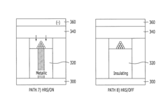
- A ReRAM is fabricated using a method where a stoichiometric transition oxide threshold switching layer and a non-stoichiometric transition metal oxide resistance change layer are formed simultaneously without sequential stacking, with the threshold switching layer comprising stoichiometric oxides like niobium or vanadium oxide, and the resistance change layer formed by oxidizing a part of the electrode, allowing for controlled resistance changes and improved read operations.
Semiconductor IP Protection Strategies
In the rapidly evolving landscape of Resistive RAM (ReRAM) technology, intellectual property protection has become a critical strategic consideration for semiconductor companies. Patent filings in this domain have increased exponentially over the past decade, with major players establishing extensive portfolios to secure their innovations. Effective IP protection strategies must address both technical innovations and market positioning to maintain competitive advantage in this high-stakes field.
Multi-layered protection approaches have proven most effective, combining patents, trade secrets, and strategic licensing agreements. Companies leading in ReRAM development typically maintain core technology patents while selectively licensing peripheral technologies to establish industry standards. This balanced approach allows for both protection of fundamental innovations and ecosystem development through controlled collaboration.
Geographic considerations play a significant role in ReRAM IP strategies. Patent filings show concentrated activity in the United States, China, South Korea, and Japan, reflecting the global manufacturing and research centers for this technology. Companies must develop region-specific protection strategies that account for varying enforcement mechanisms and legal frameworks across these jurisdictions.
The time-sensitive nature of ReRAM development necessitates accelerated patent filing strategies. Market leaders have adopted continuous filing approaches, where improvements and iterations are patented sequentially to extend protection periods and block potential competitors. This creates patent "fences" around core technologies that provide multiple layers of protection against infringement.
Cross-licensing agreements have emerged as a pragmatic solution in the fragmented ReRAM patent landscape. Major semiconductor manufacturers often negotiate these agreements to navigate the complex web of interdependent technologies, allowing continued innovation while minimizing litigation risks. These agreements frequently include field-of-use restrictions to maintain competitive boundaries.
Defensive publication strategies complement traditional patent protection by strategically disclosing non-core innovations to prevent competitors from patenting similar technologies. This approach is particularly valuable for incremental improvements that may not warrant full patent protection but could potentially block development if patented by competitors.
As ReRAM moves toward commercialization, companies are increasingly focusing on application-specific patent strategies rather than broad technology claims. This shift reflects the maturing technology landscape and the need to protect specific implementations that deliver market value in targeted applications such as edge computing, IoT devices, and neuromorphic systems.
Material Science Advancements for ReRAM
Material science innovations have been pivotal in advancing Resistive Random Access Memory (ReRAM) technology over the past decade. The fundamental challenge in ReRAM development lies in identifying and engineering materials that can reliably switch between high and low resistance states while maintaining long-term stability. Recent breakthroughs in oxide-based materials, particularly transition metal oxides like HfOx, TaOx, and TiOx, have demonstrated superior switching characteristics and compatibility with CMOS fabrication processes.
Researchers have made significant progress in understanding the role of oxygen vacancies in forming conductive filaments within these oxide layers. By precisely controlling oxygen concentration and distribution through advanced deposition techniques such as atomic layer deposition (ALD) and reactive sputtering, engineers have achieved more consistent switching behavior and reduced variability between devices.
Two-dimensional (2D) materials represent another frontier in ReRAM material science. Graphene, MoS2, and other 2D materials offer atomically thin barriers that can potentially enable ultra-low power switching mechanisms. These materials exhibit unique quantum confinement effects that may be exploited for novel switching phenomena beyond conventional filamentary mechanisms.
Interface engineering has emerged as a critical aspect of ReRAM material development. The electrode-oxide interface significantly influences switching dynamics and reliability. Noble metals (Pt, Au), reactive metals (Ti, Ta), and conducting nitrides (TiN, TaN) are being extensively studied as electrode materials to optimize charge transfer and filament formation processes at these critical interfaces.
Doping strategies have proven effective in enhancing ReRAM performance. Strategic incorporation of dopants such as Al in HfO2 or Si in TaOx has demonstrated improved retention, endurance, and switching uniformity. These dopants modify defect concentrations and energy barriers, providing finer control over switching characteristics.
Multilayer and nanocomposite structures represent another promising direction. Engineered stacks of different materials (e.g., HfO2/Al2O3 bilayers) create controlled defect profiles and energy barriers that enhance switching performance. These heterogeneous structures offer additional degrees of freedom for optimizing device characteristics beyond what single-material systems can achieve.
Advanced characterization techniques, including in-situ TEM, synchrotron-based spectroscopy, and conductive atomic force microscopy, have been instrumental in revealing the nanoscale mechanisms underlying ReRAM operation. These insights are driving rational material design approaches rather than empirical optimization, accelerating the development cycle for next-generation ReRAM materials.
Unlock deeper insights with PatSnap Eureka Quick Research — get a full tech report to explore trends and direct your research. Try now!
Generate Your Research Report Instantly with AI Agent
Supercharge your innovation with PatSnap Eureka AI Agent Platform!