Resistive RAM's Evolution in Electronics Standards Compliance
OCT 9, 20259 MIN READ
Generate Your Research Report Instantly with AI Agent
Patsnap Eureka helps you evaluate technical feasibility & market potential.
ReRAM Technology Background and Objectives
Resistive Random Access Memory (ReRAM) has emerged as a promising non-volatile memory technology over the past two decades, evolving from theoretical concepts to commercially viable products. The technology leverages the resistance switching phenomenon in certain metal oxides and other materials, where electrical resistance can be altered through the application of voltage, creating stable states that represent binary data. This fundamental principle was first observed in the 1960s, but only gained significant research momentum in the early 2000s as limitations of conventional memory technologies became increasingly apparent.
The evolution of ReRAM has been driven by the growing demands of modern computing systems that require higher density, lower power consumption, and faster operation than traditional memory technologies can provide. Flash memory, while revolutionary in its time, faces scaling limitations below 10nm nodes, while DRAM's volatility necessitates constant power for data retention. ReRAM addresses these limitations by offering non-volatility, high endurance, fast switching speeds, and compatibility with conventional CMOS processes.
Industry standards compliance represents a critical aspect of ReRAM's technological maturation. As the technology transitions from research laboratories to commercial applications, adherence to established electronics standards ensures interoperability, reliability, and market acceptance. The JEDEC Solid State Technology Association has been instrumental in developing specifications for emerging memories, including ReRAM, providing frameworks for performance metrics, reliability testing, and interface protocols.
The primary technical objectives for ReRAM development focus on several key areas. First, improving switching reliability and endurance to match or exceed that of existing memory technologies, targeting 10^12 write cycles for enterprise applications. Second, reducing operating voltages and currents to enhance energy efficiency, particularly for mobile and IoT applications. Third, increasing storage density through multi-level cell capabilities and three-dimensional architectures to compete with NAND flash in storage applications.
Additionally, ReRAM aims to address the growing need for in-memory computing architectures that can overcome the von Neumann bottleneck in data-intensive applications. By enabling computational operations directly within memory arrays, ReRAM-based systems could dramatically reduce power consumption and increase processing speed for artificial intelligence and big data analytics workloads.
The roadmap for ReRAM technology includes integration with advanced logic processes, development of specialized controllers for optimized operation, and standardization of interfaces for seamless integration into existing memory hierarchies. As the technology matures, compliance with industry standards will be paramount to ensure broad adoption across consumer electronics, enterprise storage, automotive systems, and emerging edge computing applications.
Market Demand Analysis for ReRAM Solutions
The global market for Resistive Random Access Memory (ReRAM) solutions is experiencing significant growth, driven by increasing demands for more efficient, high-performance, and low-power memory technologies. Current market projections indicate that the ReRAM market is expected to grow at a compound annual growth rate of 16% between 2023 and 2028, with the market value potentially reaching several billion dollars by the end of this forecast period.
The primary market demand for ReRAM stems from its potential to address the limitations of existing memory technologies. Traditional DRAM and NAND flash memory face scaling challenges as semiconductor devices continue to shrink, creating opportunities for alternative memory solutions like ReRAM. The non-volatile nature of ReRAM, combined with its low power consumption, high endurance, and fast switching speed, positions it as an attractive option for various applications.
In the consumer electronics sector, ReRAM is gaining traction due to its ability to enable faster boot times, reduced energy consumption, and improved overall system performance. Smartphone manufacturers are particularly interested in ReRAM for next-generation devices, as it offers the potential for instant-on functionality and extended battery life.
The Internet of Things (IoT) represents another significant market opportunity for ReRAM. The proliferation of connected devices requires memory solutions that can operate with minimal power consumption while maintaining data integrity. ReRAM's low power requirements and non-volatile characteristics make it well-suited for edge computing devices and sensors that often operate in power-constrained environments.
Data centers and enterprise storage systems are also driving demand for ReRAM solutions. As organizations process increasingly large volumes of data, there is a growing need for memory technologies that can provide faster access times and reduced latency. ReRAM's potential to bridge the performance gap between DRAM and NAND flash makes it an attractive option for storage class memory applications.
The automotive industry represents an emerging market for ReRAM, particularly with the rise of autonomous vehicles and advanced driver assistance systems. These applications require memory solutions that can withstand harsh operating conditions while providing reliable, high-speed data access. ReRAM's radiation hardness and temperature stability make it suitable for automotive applications.
Despite the promising market outlook, widespread adoption of ReRAM faces challenges related to manufacturing scalability, cost competitiveness, and standards compliance. As the technology matures and manufacturing processes improve, these barriers are expected to diminish, potentially accelerating market growth and expanding application possibilities across various industries.
ReRAM Development Status and Technical Barriers
Resistive RAM (ReRAM) technology has reached a critical juncture in its development cycle, with significant advancements achieved alongside persistent technical challenges. Current global development status indicates that ReRAM has progressed from laboratory research to early commercialization phases, with several companies including Weebit Nano, Crossbar, and Fujitsu demonstrating viable products. However, widespread adoption remains limited by several key technical barriers.
The manufacturing consistency of ReRAM devices presents a significant challenge. Current fabrication processes struggle to maintain uniform switching characteristics across large arrays, resulting in cell-to-cell variability that impacts reliability. This variability manifests as inconsistent resistance states, unpredictable switching voltages, and varying endurance characteristics, making standardization difficult for electronics compliance frameworks.
Endurance limitations constitute another major barrier. While conventional flash memory typically achieves 10^4-10^5 write cycles, ReRAM currently demonstrates endurance levels ranging from 10^6 to 10^9 cycles in laboratory settings. However, commercial implementations often fall short of these figures, particularly when operating under real-world conditions with varying temperatures and usage patterns.
Data retention capabilities present ongoing concerns for standards compliance. ReRAM devices must maintain stored information for extended periods (typically 10+ years) to meet electronics industry requirements. Current implementations show promising retention at room temperature but experience accelerated degradation at elevated temperatures, creating challenges for applications in automotive, industrial, and other harsh environments.
Integration with CMOS technology remains technically challenging. While ReRAM offers theoretical advantages for back-end-of-line integration, practical implementation requires addressing issues related to thermal budgets, material compatibility, and process contamination. These integration challenges directly impact compliance with existing semiconductor manufacturing standards.
Power consumption during write operations, particularly SET operations, continues to exceed targets for ultra-low-power applications. This limitation restricts ReRAM's potential in energy-harvesting IoT devices and other power-constrained applications where compliance with emerging low-power electronics standards is essential.
Scaling behavior represents another significant barrier. As device dimensions shrink below 20nm, ReRAM cells exhibit increased variability and reduced reliability. This scaling challenge impacts compliance with roadmaps for memory density improvements and integration with advanced logic nodes, potentially limiting ReRAM's role in next-generation computing architectures.
The lack of standardized testing methodologies specifically designed for ReRAM technology further complicates compliance efforts. Current testing frameworks, developed primarily for flash and DRAM technologies, fail to adequately characterize ReRAM's unique switching mechanisms and failure modes, creating uncertainty in reliability assessments and certification processes.
Current ReRAM Implementation Approaches
01 Industry Standards for Resistive RAM Implementation
Resistive RAM (RRAM) technologies must adhere to established industry standards to ensure interoperability and reliability. These standards govern various aspects of RRAM implementation, including interface protocols, testing methodologies, and performance benchmarks. Compliance with these standards is essential for RRAM manufacturers to ensure their products can be integrated into existing memory ecosystems and meet the expectations of system designers and end users.- Industry standards for Resistive RAM technology: Resistive RAM (RRAM) technology must comply with established industry standards to ensure interoperability and reliability. These standards govern various aspects of RRAM implementation, including memory cell architecture, interface protocols, and performance metrics. Compliance with these standards is essential for RRAM manufacturers to ensure their products can be integrated into existing systems and meet market expectations for reliability and performance.
- Testing and verification protocols for RRAM compliance: Specific testing and verification protocols are necessary to ensure that Resistive RAM devices meet required standards. These protocols include functional testing, reliability assessment, endurance testing, and performance validation. Standardized testing methodologies help in evaluating RRAM devices against established benchmarks and ensuring they meet the necessary compliance requirements before market deployment.
- Security and data protection standards for RRAM: Resistive RAM implementations must adhere to security and data protection standards to safeguard stored information. These standards address encryption requirements, access control mechanisms, and data integrity measures specific to RRAM technology. Compliance with these security standards is crucial for applications in sensitive sectors such as financial services, healthcare, and government, where data protection is paramount.
- Power consumption and energy efficiency standards: Energy efficiency standards for Resistive RAM technology establish requirements for power consumption during operation, standby, and sleep modes. These standards aim to minimize energy usage while maintaining performance, which is particularly important for battery-powered and mobile applications. RRAM devices must be designed to comply with these standards to meet market demands for energy-efficient memory solutions.
- Certification and compliance documentation for RRAM: Formal certification processes and documentation requirements exist for demonstrating Resistive RAM compliance with applicable standards. These include technical documentation, test reports, compliance declarations, and certification marks. Manufacturers must maintain comprehensive records of compliance testing and certification to satisfy regulatory requirements and customer expectations regarding standards adherence.
02 Testing and Verification Protocols for RRAM Compliance
Specific testing and verification protocols have been developed to assess RRAM compliance with industry standards. These protocols include methodologies for evaluating performance parameters such as endurance, retention, and switching speed. Verification procedures also address reliability concerns specific to resistive memory technologies, including resistance drift and variability. Standardized testing frameworks enable consistent evaluation across different RRAM implementations and facilitate certification processes.Expand Specific Solutions03 Security and Data Protection Standards for RRAM
Security standards for RRAM address data protection requirements and secure operation in various applications. These standards define protocols for secure data storage, encryption capabilities, and protection against unauthorized access or tampering. As RRAM is increasingly used in security-sensitive applications, compliance with these standards becomes critical for ensuring data integrity and confidentiality. The standards also cover secure erase procedures and protection against side-channel attacks specific to resistive memory technologies.Expand Specific Solutions04 Power and Performance Standards for RRAM Devices
Power consumption and performance standards for RRAM establish benchmarks for energy efficiency, speed, and operational characteristics. These standards define acceptable ranges for parameters such as read/write latency, power consumption during different operational modes, and performance degradation over time. Compliance with these standards ensures that RRAM devices meet the requirements for various applications, from low-power IoT devices to high-performance computing systems. The standards also address thermal management considerations specific to resistive memory technologies.Expand Specific Solutions05 Integration and Compatibility Standards for RRAM Systems
Integration standards for RRAM define requirements for compatibility with existing memory hierarchies and system architectures. These standards address interface specifications, signal timing, command structures, and physical form factors to ensure RRAM can be incorporated into diverse computing platforms. Compliance with these integration standards facilitates the adoption of RRAM technology by ensuring compatibility with established memory controllers and system software. The standards also cover migration paths from traditional memory technologies to RRAM-based solutions.Expand Specific Solutions
Key Industry Players in ReRAM Development
Resistive RAM technology is currently in a transitional phase from research to early commercialization, with the global market expected to reach $2-3 billion by 2025. The competitive landscape features established semiconductor giants like Samsung, Intel, and TSMC investing heavily in ReRAM development alongside specialized players such as CrossBar and Adesto Technologies. Technical maturity varies significantly across implementations, with companies like Winbond, Macronix, and SK hynix focusing on embedded ReRAM solutions for specific applications, while IBM and Toshiba are advancing 3D crossbar architectures for higher density storage. Standards compliance remains a challenge as companies balance proprietary innovations with interoperability requirements, particularly for automotive and industrial applications where reliability standards are stringent.
Taiwan Semiconductor Manufacturing Co., Ltd.
Technical Solution: TSMC has developed embedded Resistive RAM (eReRAM) technology as part of their advanced logic process nodes. Their implementation utilizes a hafnium oxide-based switching layer integrated into the back-end-of-line (BEOL) process, allowing for seamless integration with logic circuits. TSMC's eReRAM technology complies with JEDEC JEP122 standards for failure mechanisms and models in semiconductor devices, and their qualification methodology follows JEDEC JESD47 standards for stress-test-driven qualification. The company has demonstrated eReRAM modules with 10^5 endurance cycles and retention exceeding 10 years at 85°C. TSMC's eReRAM technology has been designed to meet AEC-Q100 automotive electronics reliability standards and IEC 61508 functional safety requirements. Their embedded memory solutions support standardized interfaces including AMBA APB for peripheral bus connectivity and SRAM-like interfaces for direct CPU access, ensuring compatibility with existing system architectures.
Strengths: Industry-leading manufacturing processes allowing for tight integration with logic; established quality control systems ensuring high reliability and yield. Weaknesses: Limited to embedded applications rather than standalone memory products; higher cost structure compared to dedicated memory manufacturers.
KIOXIA Corp.
Technical Solution: KIOXIA (formerly Toshiba Memory) has developed a proprietary ReRAM technology based on a metal oxide switching material utilizing a filamentary conduction mechanism. Their implementation features a crosspoint architecture that enables high-density storage with multi-layer stacking capabilities. KIOXIA's ReRAM technology complies with JEDEC JC-64.8 standards for solid-state drive requirements and JESD218 reliability qualification requirements. The company has demonstrated ReRAM devices with endurance exceeding 10^7 cycles and data retention of over 10 years at 85°C. KIOXIA has focused on ensuring their ReRAM solutions meet the TCG Opal Security Subsystem Class specifications for data security and the NVMe standard for interface compatibility. Their technology roadmap includes development of ReRAM solutions compliant with emerging CXL (Compute Express Link) standards and PCIe Gen5 specifications to support high-bandwidth memory applications in data centers and enterprise storage systems.
Strengths: Strong expertise in memory controller design optimized for ReRAM characteristics; established relationships with major OEMs for product qualification. Weaknesses: Relatively higher manufacturing costs compared to conventional NAND flash; temperature sensitivity requiring additional compensation circuits.
Critical ReRAM Patents and Technical Innovations
NAND array comprising parallel transistor and two-terminal switching device
PatentWO2015130699A1
Innovation
- A NAND architecture featuring a 1 transistor - 1 two-terminal memory device (IT-ID) arrangement with memory cells connected in parallel, utilizing resistive memory devices or other two-terminal technologies like ferromagnetic or phase change memory, which allows for faster write and erase times, improved data longevity, and reduced bit errors by minimizing capacitance and enabling selective control of memory operations.


Multi-level resistive memory structure
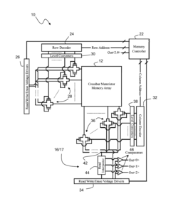
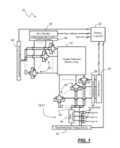
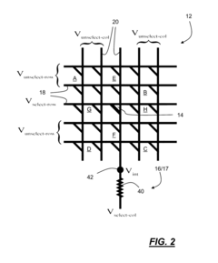
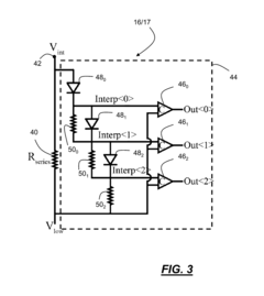
PatentActiveUS20170140815A1
Innovation
- A resistive memory structure with an interpretation circuit that includes active and passive devices connected in series to interpret voltage levels at an electrical node, allowing for accurate determination of resistive states without significant peripheral circuitry, and a method involving specific voltage biasing schemes to minimize resistance changes during operations.
Standards Compliance Framework for ReRAM Integration
The integration of Resistive RAM (ReRAM) into mainstream electronics requires adherence to a comprehensive standards compliance framework. This framework encompasses multiple layers of standardization, beginning with basic electrical specifications that define voltage ranges, current limits, and timing parameters essential for ReRAM operation within diverse electronic systems. These specifications ensure interoperability across different hardware platforms while maintaining performance consistency.
Physical interface standards constitute another critical component, defining pin configurations, form factors, and connection protocols. For ReRAM technologies, these standards must accommodate both traditional memory interfaces and emerging neuromorphic computing applications, requiring flexibility in physical implementation while maintaining backward compatibility with existing systems.
Data communication protocols represent the third layer of the framework, establishing how information is transferred to and from ReRAM devices. These protocols must address ReRAM's unique characteristics, including variable resistance states, non-volatile storage capabilities, and potential analog computing functions, while remaining compatible with established digital communication standards.
Testing and validation methodologies form a crucial element of the compliance framework, providing standardized procedures for verifying ReRAM performance, reliability, and endurance. These methodologies include accelerated aging tests, data retention assessments, and resistance drift measurements specific to ReRAM technology, enabling consistent quality evaluation across manufacturers and applications.
Industry certification processes constitute the framework's verification mechanism, offering formal recognition of compliance with established standards. For ReRAM, these processes are evolving to incorporate specialized testing for emerging applications in edge computing, IoT devices, and artificial intelligence accelerators, where ReRAM's low power consumption and non-volatile characteristics offer significant advantages.
Regulatory compliance requirements complete the framework, addressing safety, electromagnetic compatibility, and environmental considerations. These requirements vary by region and application domain, necessitating a flexible approach to ReRAM implementation that can adapt to diverse regulatory landscapes while maintaining core functionality and performance characteristics.
The standards compliance framework for ReRAM integration continues to evolve as the technology matures, with industry consortia and standards organizations actively developing new specifications that balance innovation with interoperability, ensuring ReRAM can fulfill its potential across multiple electronic domains while maintaining necessary compatibility with existing systems and future technologies.
Environmental Impact of ReRAM Manufacturing
The manufacturing processes of Resistive Random Access Memory (ReRAM) present both environmental challenges and opportunities compared to conventional memory technologies. ReRAM fabrication typically involves fewer process steps than traditional NAND flash memory, potentially reducing overall energy consumption and chemical usage. Studies indicate that ReRAM manufacturing can achieve up to 30% reduction in carbon footprint compared to equivalent DRAM or flash memory production, primarily due to simplified layer deposition processes and reduced thermal budget requirements.
However, ReRAM production still involves several environmentally concerning aspects. The metal oxide layers central to ReRAM operation often contain rare earth elements or transition metals such as hafnium, titanium, and tantalum. Mining and processing these materials generate significant environmental impacts, including habitat destruction, water pollution, and high energy consumption. Additionally, some ReRAM variants utilize potentially toxic materials like heavy metals that require careful handling during manufacturing and proper disposal at end-of-life.
Water usage represents another critical environmental consideration in ReRAM fabrication. While generally lower than in conventional semiconductor manufacturing, ReRAM production still requires ultra-pure water for cleaning and processing steps. A typical ReRAM fabrication facility may consume thousands of gallons of water daily, contributing to water scarcity concerns in manufacturing regions.
Recent advancements in green manufacturing techniques are gradually improving ReRAM's environmental profile. Several leading manufacturers have implemented closed-loop water recycling systems that reduce freshwater consumption by up to 60%. Material innovation has also enabled partial substitution of rare earth elements with more abundant alternatives, though performance trade-offs remain a challenge in these environmentally optimized designs.
Energy efficiency during manufacturing has seen notable improvements through process optimization. Low-temperature deposition techniques have reduced the thermal energy requirements for ReRAM fabrication by approximately 25% compared to earlier generation processes. Additionally, the transition to larger wafer sizes (300mm becoming standard) has improved manufacturing efficiency, allowing more devices to be produced per unit of energy and materials consumed.
Waste management protocols specific to ReRAM manufacturing have evolved to address the unique chemical composition of production byproducts. Advanced filtration systems now capture over 95% of metal particulates from waste streams, preventing their release into the environment. However, end-of-life recycling remains underdeveloped, with less than 15% of critical materials currently recovered from discarded ReRAM devices.
Unlock deeper insights with Patsnap Eureka Quick Research — get a full tech report to explore trends and direct your research. Try now!
Generate Your Research Report Instantly with AI Agent
Supercharge your innovation with Patsnap Eureka AI Agent Platform!