Resistive RAM Technology and Its Regulatory Implications
OCT 9, 20259 MIN READ
Generate Your Research Report Instantly with AI Agent
PatSnap Eureka helps you evaluate technical feasibility & market potential.
RRAM Technology Evolution and Objectives
Resistive Random Access Memory (RRAM) technology has evolved significantly since its conceptual introduction in the 1960s. The fundamental principle of RRAM relies on the reversible change in resistance of a dielectric material when subjected to electrical stress, creating a non-volatile memory effect. This resistance-switching phenomenon enables data storage without requiring constant power, positioning RRAM as a promising candidate for next-generation memory solutions.
The evolution of RRAM technology can be traced through several key developmental phases. Initial research focused on understanding the basic resistance switching mechanisms in metal oxides. By the early 2000s, researchers had demonstrated functional RRAM devices using various material systems, including transition metal oxides such as TiO2, HfO2, and Ta2O5. These early prototypes established the viability of RRAM as a potential memory technology.
Significant technological breakthroughs occurred between 2010 and 2015, when researchers achieved improved switching reliability, reduced operating voltages, and enhanced endurance characteristics. This period saw the emergence of various RRAM architectures, including filamentary and interface-type switching mechanisms, each offering distinct advantages for specific applications.
The current technological landscape shows RRAM advancing toward commercial viability, with major semiconductor companies investing in research and development. Recent innovations have focused on addressing key challenges such as device variability, retention characteristics, and scaling limitations. Multi-level cell capabilities have also been demonstrated, potentially increasing storage density and expanding application possibilities.
The primary objectives of RRAM technology development center on creating memory solutions that combine the speed of SRAM, the density of DRAM, and the non-volatility of flash memory. Specific technical goals include reducing operating voltages below 1V, achieving endurance cycles exceeding 10^12, ensuring data retention periods of over 10 years, and enabling sub-10nm feature sizes for high-density integration.
From a regulatory perspective, RRAM development aims to comply with international standards for electronic components while addressing emerging concerns related to data security and privacy. As RRAM potentially enables new computing paradigms such as in-memory computing and neuromorphic applications, regulatory frameworks may need to evolve to accommodate these novel architectures.
Looking forward, RRAM technology is expected to continue its trajectory toward becoming a mainstream memory solution, particularly for applications requiring low power consumption, high speed, and non-volatility. The technology's potential to enable edge computing devices, Internet of Things (IoT) nodes, and artificial intelligence accelerators aligns with broader industry trends toward distributed computing architectures and energy-efficient electronics.
Market Demand Analysis for Non-Volatile Memory Solutions
The non-volatile memory (NVM) market is experiencing significant growth driven by increasing data storage demands across multiple sectors. Current market analysis indicates that the global NVM market is projected to reach $82 billion by 2025, with a compound annual growth rate of approximately 10.2% from 2020. This growth trajectory is primarily fueled by the expanding applications in consumer electronics, automotive systems, enterprise storage, and emerging IoT devices.
Resistive RAM (ReRAM) technology is positioned to capture a substantial portion of this expanding market due to its superior performance characteristics compared to traditional memory solutions. Industry reports suggest that ReRAM could potentially address 15-20% of the total NVM market by 2027, representing a significant opportunity for technology developers and manufacturers.
The demand for ReRAM is particularly strong in data-intensive applications where power efficiency and speed are critical factors. Cloud computing infrastructure providers are increasingly seeking memory solutions that can reduce energy consumption while maintaining high performance, with some major providers reporting that memory operations account for up to 30% of their data center power usage.
Consumer electronics manufacturers are another key demand driver, with smartphones and tablets requiring memory solutions that balance performance with battery life. Market surveys indicate that approximately 65% of consumers consider battery life a critical factor in purchasing decisions, creating a strong incentive for manufacturers to adopt more efficient memory technologies like ReRAM.
The automotive sector represents a rapidly growing market segment for ReRAM technology. Advanced driver-assistance systems (ADAS) and autonomous vehicles require robust, high-performance memory solutions capable of operating in extreme conditions. Industry forecasts predict that the automotive memory market will grow at 15% annually through 2026, with ReRAM well-positioned to capture market share due to its radiation hardness and temperature stability.
Industrial IoT applications present another significant market opportunity. Manufacturing, logistics, and utility companies are deploying increasing numbers of connected sensors and edge computing devices, creating demand for memory solutions that combine low power consumption with high reliability. Market research indicates that industrial IoT deployments are growing at 22% annually, with memory components representing a critical enabling technology.
Healthcare and medical devices represent an emerging but potentially lucrative market for ReRAM technology. Medical imaging equipment, implantable devices, and point-of-care diagnostic tools all benefit from ReRAM's combination of speed, endurance, and low power consumption. Regulatory requirements in healthcare create high barriers to entry but also support premium pricing for qualified memory solutions.
RRAM Development Status and Technical Barriers
Resistive RAM (RRAM) technology has reached a critical development stage with significant advancements in recent years. Currently, RRAM devices demonstrate promising characteristics including low power consumption, high-speed operation, excellent scalability, and compatibility with CMOS processes. Leading research institutions and semiconductor companies have achieved switching speeds in the nanosecond range, endurance cycles exceeding 10^9, and retention times of over 10 years at elevated temperatures, positioning RRAM as a viable candidate for next-generation non-volatile memory applications.
Despite these achievements, RRAM faces several substantial technical barriers that impede its widespread commercial adoption. The most significant challenge remains the device-to-device and cycle-to-cycle variability, which affects reliability and yield in mass production. This variability stems from the stochastic nature of filament formation and rupture processes that govern RRAM operation, creating inconsistencies in switching parameters across devices and operational cycles.
Another critical barrier is the sneak path current issue in crossbar array architectures, which causes interference between adjacent memory cells and limits array density. While selector devices have been proposed as solutions, integrating these components without compromising performance or increasing manufacturing complexity remains challenging. The trade-off between retention and switching voltage also presents a fundamental obstacle, as improving data retention typically requires higher operating voltages, contradicting the low-power operation goal.
Material stability represents another significant hurdle, particularly regarding the degradation of switching characteristics over time due to ion migration and interface reactions. This affects the long-term reliability of RRAM devices and their performance under various environmental conditions. Additionally, the scaling behavior of RRAM cells below 10nm node raises concerns about quantum effects potentially disrupting the conventional switching mechanisms.
From a manufacturing perspective, RRAM faces integration challenges with standard CMOS processes, particularly regarding thermal budget constraints and material compatibility issues. The industry still lacks standardized testing protocols and reliability models specifically tailored for RRAM technology, making quality assessment and failure analysis difficult to standardize across different manufacturers.
Regulatory barriers further complicate RRAM development, with varying international standards for emerging memory technologies creating compliance challenges for global deployment. Intellectual property fragmentation across multiple companies and research institutions has resulted in a complex patent landscape that may impede technology transfer and commercialization efforts.
The geographical distribution of RRAM technology development shows concentration in East Asia (particularly Japan, South Korea, and Taiwan), the United States, and Europe, with each region focusing on different aspects of the technology based on their industrial strengths and research priorities.
Current RRAM Implementation Approaches
01 ReRAM device structures and fabrication methods
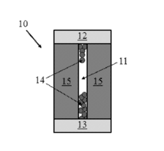
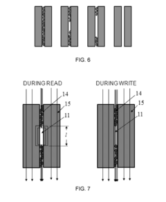
Resistive RAM (ReRAM) devices can be fabricated using various structures and methods to enhance performance and reliability. These include multi-layer structures with specific electrode materials, resistive switching layers, and barrier layers. Advanced fabrication techniques such as atomic layer deposition, physical vapor deposition, and lithography processes are employed to create these structures with precise control over dimensions and interfaces, which are critical for reliable switching behavior and device longevity.- ReRAM device structures and fabrication methods: Various device structures and fabrication methods for Resistive RAM (ReRAM) have been developed to enhance performance and reliability. These include specific electrode configurations, integration of novel materials, and specialized deposition techniques. The structures often incorporate transition metal oxides as the switching layer between conductive electrodes. Advanced fabrication methods focus on controlling the formation of conductive filaments that enable the resistive switching mechanism.
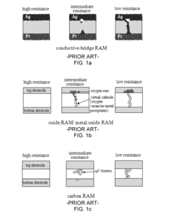
- Switching mechanisms and materials for ReRAM: The resistive switching mechanism in ReRAM relies on the formation and rupture of conductive filaments within the switching layer. Various materials have been investigated for this purpose, including metal oxides, chalcogenides, and perovskites. The selection of materials significantly impacts the switching characteristics, endurance, and retention time of ReRAM devices. Research focuses on understanding and controlling the physical and chemical processes that govern the resistive switching behavior.
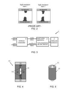
- Integration of ReRAM in memory architectures: ReRAM can be integrated into various memory architectures to leverage its advantages of high density, low power consumption, and non-volatility. These architectures include crossbar arrays, 3D stacking, and hybrid memory systems. Integration challenges involve addressing issues such as sneak path currents, selector devices, and peripheral circuitry design. Advanced memory architectures aim to optimize the trade-offs between density, speed, and reliability.
- ReRAM for neuromorphic computing applications: ReRAM devices are being developed for neuromorphic computing applications due to their ability to mimic synaptic behavior. The analog resistance modulation in ReRAM cells can represent synaptic weights in artificial neural networks. This enables efficient implementation of learning algorithms and parallel processing capabilities. Neuromorphic systems based on ReRAM offer potential advantages in terms of energy efficiency and computational density compared to conventional computing architectures.
- Reliability and performance enhancement techniques: Various techniques have been developed to enhance the reliability and performance of ReRAM devices. These include pulse engineering for programming operations, interface engineering to control ion migration, and doping strategies to modify the switching layer properties. Additional approaches focus on addressing issues such as variability, endurance degradation, and retention loss. These techniques aim to improve the overall stability and consistency of ReRAM operation for commercial applications.
02 Materials for ReRAM switching layers
The selection of materials for the resistive switching layer is crucial for ReRAM performance. Various materials including metal oxides (such as HfOx, TaOx, TiOx), chalcogenides, and perovskites exhibit resistive switching behavior suitable for ReRAM applications. These materials can be doped or combined with other elements to tune their switching characteristics, retention time, and endurance. The interface between the switching layer and electrodes plays a significant role in determining the switching mechanism and overall device performance.Expand Specific Solutions03 ReRAM array architecture and integration
ReRAM cells can be organized in various array architectures to optimize density, access speed, and power consumption. These include crossbar arrays, 3D stacked structures, and hybrid architectures that combine ReRAM with conventional memory or logic devices. Integration challenges such as sneak path current mitigation, selector device implementation, and peripheral circuit design are addressed through innovative circuit techniques and device structures to enable high-density memory arrays with reliable operation.Expand Specific Solutions04 Switching mechanisms and reliability enhancement
Understanding and controlling the resistive switching mechanisms in ReRAM is essential for improving device reliability. Various mechanisms including filamentary conduction, interface-type switching, and valence change have been identified. Techniques to enhance reliability include optimizing programming algorithms, implementing multi-level cell operation, and developing strategies to mitigate issues such as retention loss, endurance degradation, and variability. These approaches help extend device lifetime and ensure consistent performance under various operating conditions.Expand Specific Solutions05 ReRAM applications and emerging technologies
ReRAM technology extends beyond conventional memory applications to emerging fields such as neuromorphic computing, in-memory computing, and edge AI. The analog nature of resistive switching makes ReRAM suitable for implementing artificial neural networks and synaptic functions. Additionally, ReRAM is being explored for security applications like physical unclonable functions (PUFs) and true random number generators. Integration with other emerging technologies such as 2D materials, flexible substrates, and quantum computing platforms represents the frontier of ReRAM research and development.Expand Specific Solutions
Leading RRAM Industry Players and Ecosystem
Resistive RAM (RRAM) technology is currently in the early growth phase of its industry lifecycle, with the market expected to expand significantly due to increasing demand for high-performance, low-power memory solutions. The global RRAM market, valued at approximately $310 million in 2022, is projected to reach $2.6 billion by 2028, representing a CAGR of over 35%. Technologically, RRAM is approaching maturity with key players advancing commercial viability. Samsung Electronics, Micron Technology, and KIOXIA lead in patent portfolios and manufacturing capabilities, while specialized companies like CrossBar and Hefei Reliance Memory focus on innovative RRAM architectures. Traditional memory manufacturers including Winbond, TSMC, and UMC are investing heavily in RRAM research, while research institutions such as ITRI and GIST contribute fundamental technological breakthroughs that address remaining challenges in endurance and reliability.
Samsung Electronics Co., Ltd.
Technical Solution: Samsung has developed an advanced ReRAM technology utilizing a metal-oxide switching layer (typically HfO2 or Ta2O5) that creates and dissolves conductive filaments through oxygen vacancy manipulation. Their ReRAM architecture integrates with their established manufacturing processes, enabling high-yield production. Samsung's implementation achieves switching speeds below 10ns with power consumption under 10pJ per operation. The company has demonstrated ReRAM cells with endurance exceeding 10^6 cycles and retention times over 10 years at 85°C. Samsung has focused on optimizing their ReRAM for neuromorphic computing applications, leveraging the analog conductance states to implement artificial synapses. Their technology roadmap includes integration of ReRAM with logic circuits in 3D stacked configurations to enable in-memory computing architectures that dramatically reduce data movement and power consumption.
Strengths: Massive manufacturing infrastructure and expertise; integration capabilities with existing product lines; strong IP portfolio in ReRAM technology. Weaknesses: Competing internal memory technologies (DRAM, NAND, MRAM) may limit resource allocation to ReRAM development; conservative approach to market introduction of new memory technologies.
Micron Technology, Inc.
Technical Solution: Micron's ReRAM technology employs a hafnium oxide-based switching layer with proprietary electrode materials that optimize filament formation and dissolution. Their 3D architecture enables vertical stacking of memory cells, significantly increasing storage density while maintaining CMOS compatibility. Micron has demonstrated ReRAM cells with sub-10ns switching speeds, endurance exceeding 10^9 cycles, and data retention of over 10 years at 85°C. Their technology achieves write operations at approximately 3pJ per bit, substantially lower than conventional flash memory. Micron has focused on optimizing their ReRAM for both discrete memory applications and embedded solutions, particularly targeting IoT and automotive markets where power efficiency and reliability in harsh environments are critical. Their manufacturing approach leverages existing fab infrastructure with minimal process modifications, enabling cost-effective production scaling.
Strengths: Extensive memory manufacturing expertise; strong materials science capabilities; well-established global supply chain and customer relationships. Weaknesses: Competing internal priorities across multiple memory technologies; challenges in achieving cost parity with established memory types at high volumes.
Key RRAM Materials and Switching Mechanism Patents
Resistive random access memory
PatentActiveUS20200266344A1
Innovation
- Incorporating two variable resistance layers between the lower and upper electrodes, allowing for multiple resistance states and improved material selection to enhance the current on/off ratio and maintain threshold voltage, thereby increasing storage density and data retention.
Resistive random-access memory cells
PatentActiveUS20160196874A1
Innovation
- The introduction of an electrically-conductive component within the RRAM cell structure, which allows for programmable cell states by varying the resistance of the conductive path and insulating matrix, enabling effective differentiation of high-resistance states and reducing sneak-path currents without destructive read operations.
Regulatory Framework for Emerging Memory Technologies
The regulatory landscape for emerging memory technologies like Resistive RAM (ReRAM) is evolving rapidly as these technologies move from research laboratories to commercial applications. Current regulatory frameworks primarily focus on traditional semiconductor technologies and often lack specific provisions for novel memory architectures. This regulatory gap creates uncertainty for manufacturers, investors, and end-users of ReRAM technology.
At the international level, organizations such as the International Electrotechnical Commission (IEC) and the Institute of Electrical and Electronics Engineers (IEEE) are developing standards that will eventually govern ReRAM implementation. These standards address performance metrics, reliability parameters, and testing methodologies specific to resistive switching mechanisms. However, the pace of standardization lags behind technological advancement, creating potential barriers to market entry.
Data security regulations present another critical dimension for ReRAM deployment. As these memory technologies potentially store sensitive information in new ways, existing data protection frameworks like GDPR in Europe and CCPA in California may require interpretation or amendment to address ReRAM-specific vulnerabilities or capabilities. The non-volatile nature of ReRAM raises particular concerns about data persistence and secure erasure protocols.
Environmental regulations also impact ReRAM development and commercialization. While ReRAM potentially offers lower power consumption than conventional memory technologies, the materials used in some ReRAM implementations may fall under restrictions imposed by regulations such as RoHS (Restriction of Hazardous Substances) or REACH (Registration, Evaluation, Authorization and Restriction of Chemicals). Manufacturers must navigate these requirements while optimizing device performance.
Intellectual property protection represents another regulatory challenge. The patent landscape for ReRAM is increasingly complex, with overlapping claims from academic institutions, established semiconductor companies, and startups. Regulatory bodies like the USPTO and EPO are still developing approaches to evaluate novelty and non-obviousness in this rapidly evolving field.
Export control regulations add further complexity, particularly for dual-use technologies with potential military applications. ReRAM's radiation hardness and potential use in aerospace or defense systems may trigger restrictions under frameworks like the Wassenaar Arrangement or country-specific export control regimes. Companies developing ReRAM must implement compliance programs to navigate these restrictions.
Looking forward, regulatory frameworks will need to balance innovation encouragement with appropriate safeguards. Industry-government collaboration will be essential to develop regulations that address legitimate concerns without unnecessarily impeding technological progress in this promising field.
Energy Efficiency and Sustainability Aspects of RRAM
Resistive RAM (RRAM) technology presents significant advantages in energy efficiency compared to conventional memory technologies. RRAM devices operate on the principle of resistance switching, requiring substantially lower programming voltages (typically 1-3V) than flash memory (10-20V), resulting in reduced power consumption during write operations. The non-volatile nature of RRAM eliminates the need for constant power to maintain stored data, making it particularly valuable for energy-constrained applications such as IoT devices and mobile computing.
From a sustainability perspective, RRAM manufacturing processes potentially offer reduced environmental impact compared to traditional semiconductor memory fabrication. The simpler structure of RRAM cells requires fewer processing steps and potentially less toxic materials. Additionally, the compatibility with back-end-of-line (BEOL) processing allows for three-dimensional integration, maximizing silicon utilization and reducing the overall material footprint per bit of storage.
The extended endurance capabilities of RRAM technology—with some variants demonstrating up to 10^12 write cycles—significantly outperform flash memory's typical 10^4-10^5 cycles. This longevity translates directly to sustainability benefits through reduced electronic waste generation, as devices require less frequent replacement due to memory degradation.
Power consumption analysis reveals that RRAM arrays can achieve standby power as low as nanowatts, compared to microwatts for conventional DRAM. During active operations, RRAM demonstrates energy efficiency of approximately 0.1-1 pJ per bit operation, representing a 10-100x improvement over flash memory technologies in certain applications.
Regulatory frameworks are beginning to acknowledge these sustainability advantages. The European Union's Ecodesign Directive and Energy Star specifications are evolving to incorporate emerging memory technologies like RRAM. Manufacturers implementing RRAM may gain competitive advantages through compliance with increasingly stringent energy efficiency regulations and carbon footprint reduction targets.
However, challenges remain in fully realizing RRAM's sustainability potential. Current fabrication processes still utilize some rare earth materials and potentially hazardous substances. Future regulatory developments may impose stricter requirements on material sourcing and end-of-life recycling for RRAM-based products, necessitating continued innovation in environmentally friendly manufacturing techniques and materials selection.
Unlock deeper insights with PatSnap Eureka Quick Research — get a full tech report to explore trends and direct your research. Try now!
Generate Your Research Report Instantly with AI Agent
Supercharge your innovation with PatSnap Eureka AI Agent Platform!