

The Semiconductor Industry’s Shift Towards Resistive RAM
OCT 9, 20259 MIN READ
Generate Your Research Report Instantly with AI Agent
PatSnap Eureka helps you evaluate technical feasibility & market potential.
ReRAM Technology Evolution and Objectives
Resistive Random Access Memory (ReRAM) represents a significant paradigm shift in semiconductor memory technology, emerging as a promising alternative to conventional memory solutions. The evolution of ReRAM can be traced back to the early 2000s when researchers began exploring the potential of resistance-based memory cells. This technology leverages the unique property of certain materials to change their resistance states when subjected to electrical stimuli, enabling data storage through resistance variations rather than electrical charge.
The development trajectory of ReRAM has been characterized by progressive improvements in material science, fabrication techniques, and circuit design. Initially, metal oxide-based ReRAM structures demonstrated the fundamental concept but suffered from reliability issues and limited endurance. Subsequent advancements in material engineering, particularly the introduction of hafnium oxide and tantalum oxide-based structures, significantly enhanced performance metrics, establishing ReRAM as a viable memory technology.
Current technical objectives for ReRAM development focus on addressing several critical challenges. Foremost among these is scaling capability, as the semiconductor industry continues its relentless pursuit of higher density memory solutions. ReRAM's inherent simplicity in cell structure theoretically allows for aggressive scaling beyond the limitations of conventional flash memory, potentially enabling sub-10nm node implementation.
Another primary objective involves enhancing operational reliability and endurance. While ReRAM offers promising write/erase cycles compared to flash memory, achieving the stability required for enterprise and automotive applications remains a significant technical hurdle. Researchers are actively exploring novel material compositions and interface engineering to mitigate issues such as resistance drift and retention degradation.
Power efficiency represents another crucial development goal. The non-volatile nature of ReRAM inherently reduces standby power consumption, but optimizing active power requirements during write operations continues to be a focus area. This is particularly relevant for battery-powered applications where energy efficiency directly impacts user experience.
Integration compatibility with existing CMOS processes constitutes a fundamental objective for commercial viability. The ability to fabricate ReRAM cells using standard semiconductor manufacturing equipment and processes significantly reduces implementation barriers and accelerates market adoption. Current research emphasizes back-end-of-line integration approaches that minimize disruption to established fabrication workflows.
The semiconductor industry's strategic pivot toward ReRAM is further driven by its potential to enable novel computing paradigms. In-memory computing and neuromorphic applications leverage ReRAM's analog resistance states to perform computational tasks directly within memory arrays, potentially revolutionizing data-intensive applications like artificial intelligence and machine learning.
The development trajectory of ReRAM has been characterized by progressive improvements in material science, fabrication techniques, and circuit design. Initially, metal oxide-based ReRAM structures demonstrated the fundamental concept but suffered from reliability issues and limited endurance. Subsequent advancements in material engineering, particularly the introduction of hafnium oxide and tantalum oxide-based structures, significantly enhanced performance metrics, establishing ReRAM as a viable memory technology.
Current technical objectives for ReRAM development focus on addressing several critical challenges. Foremost among these is scaling capability, as the semiconductor industry continues its relentless pursuit of higher density memory solutions. ReRAM's inherent simplicity in cell structure theoretically allows for aggressive scaling beyond the limitations of conventional flash memory, potentially enabling sub-10nm node implementation.
Another primary objective involves enhancing operational reliability and endurance. While ReRAM offers promising write/erase cycles compared to flash memory, achieving the stability required for enterprise and automotive applications remains a significant technical hurdle. Researchers are actively exploring novel material compositions and interface engineering to mitigate issues such as resistance drift and retention degradation.
Power efficiency represents another crucial development goal. The non-volatile nature of ReRAM inherently reduces standby power consumption, but optimizing active power requirements during write operations continues to be a focus area. This is particularly relevant for battery-powered applications where energy efficiency directly impacts user experience.
Integration compatibility with existing CMOS processes constitutes a fundamental objective for commercial viability. The ability to fabricate ReRAM cells using standard semiconductor manufacturing equipment and processes significantly reduces implementation barriers and accelerates market adoption. Current research emphasizes back-end-of-line integration approaches that minimize disruption to established fabrication workflows.
The semiconductor industry's strategic pivot toward ReRAM is further driven by its potential to enable novel computing paradigms. In-memory computing and neuromorphic applications leverage ReRAM's analog resistance states to perform computational tasks directly within memory arrays, potentially revolutionizing data-intensive applications like artificial intelligence and machine learning.
Market Demand Analysis for Next-Gen Memory Solutions
The global memory market is experiencing a significant transformation driven by emerging technologies and evolving application requirements. Current projections indicate the next-generation memory market will reach approximately $20 billion by 2028, with Resistive RAM (ReRAM) positioned as a key growth segment. This surge is primarily fueled by increasing demands for higher performance, lower power consumption, and greater storage density across multiple industries.
Data centers represent the largest market segment for advanced memory solutions, as they face mounting pressure to process exponentially growing data volumes while minimizing energy consumption. The artificial intelligence and machine learning sectors follow closely, requiring memory architectures that can support massive parallel processing operations with minimal latency. These applications demand memory solutions that overcome the limitations of traditional DRAM and NAND flash technologies.
Consumer electronics manufacturers are actively seeking memory technologies that extend battery life while maintaining or improving performance. Market research indicates that smartphones, tablets, and wearable devices collectively account for approximately 35% of potential ReRAM applications, with consumers increasingly prioritizing devices that offer longer usage times between charges.
The automotive sector presents another substantial growth opportunity, particularly with the advancement of autonomous vehicles. These systems require memory solutions capable of rapid data processing in harsh environmental conditions while maintaining absolute reliability. Industry analysts project that automotive memory requirements will grow at a compound annual rate of 25% through 2027, significantly outpacing most other sectors.
Industrial IoT applications represent an emerging but rapidly expanding market segment. The deployment of edge computing solutions across manufacturing, logistics, and infrastructure monitoring creates demand for memory technologies that combine durability, energy efficiency, and cost-effectiveness. This sector is expected to generate substantial demand for ReRAM solutions as IoT deployments scale globally.
From a geographical perspective, Asia-Pacific currently leads in memory technology adoption, accounting for approximately 45% of the global market. North America follows at 30%, with particularly strong demand from data center operators and AI research institutions. European markets contribute approximately 20%, with emphasis on automotive and industrial applications.
Market research indicates that customers across all segments are willing to pay premium prices for memory solutions that deliver meaningful improvements in three key areas: power efficiency, data retention reliability, and processing speed. ReRAM technology addresses these priorities by offering non-volatile storage with faster write speeds than flash memory and significantly lower power consumption than DRAM, positioning it favorably against competing next-generation memory technologies.
Data centers represent the largest market segment for advanced memory solutions, as they face mounting pressure to process exponentially growing data volumes while minimizing energy consumption. The artificial intelligence and machine learning sectors follow closely, requiring memory architectures that can support massive parallel processing operations with minimal latency. These applications demand memory solutions that overcome the limitations of traditional DRAM and NAND flash technologies.
Consumer electronics manufacturers are actively seeking memory technologies that extend battery life while maintaining or improving performance. Market research indicates that smartphones, tablets, and wearable devices collectively account for approximately 35% of potential ReRAM applications, with consumers increasingly prioritizing devices that offer longer usage times between charges.
The automotive sector presents another substantial growth opportunity, particularly with the advancement of autonomous vehicles. These systems require memory solutions capable of rapid data processing in harsh environmental conditions while maintaining absolute reliability. Industry analysts project that automotive memory requirements will grow at a compound annual rate of 25% through 2027, significantly outpacing most other sectors.
Industrial IoT applications represent an emerging but rapidly expanding market segment. The deployment of edge computing solutions across manufacturing, logistics, and infrastructure monitoring creates demand for memory technologies that combine durability, energy efficiency, and cost-effectiveness. This sector is expected to generate substantial demand for ReRAM solutions as IoT deployments scale globally.
From a geographical perspective, Asia-Pacific currently leads in memory technology adoption, accounting for approximately 45% of the global market. North America follows at 30%, with particularly strong demand from data center operators and AI research institutions. European markets contribute approximately 20%, with emphasis on automotive and industrial applications.
Market research indicates that customers across all segments are willing to pay premium prices for memory solutions that deliver meaningful improvements in three key areas: power efficiency, data retention reliability, and processing speed. ReRAM technology addresses these priorities by offering non-volatile storage with faster write speeds than flash memory and significantly lower power consumption than DRAM, positioning it favorably against competing next-generation memory technologies.
ReRAM Development Status and Technical Barriers
ReRAM (Resistive Random Access Memory) technology has emerged as a promising next-generation non-volatile memory solution, positioned between conventional DRAM and NAND flash in the memory hierarchy. Current development status shows significant progress in material science and fabrication techniques, with several major semiconductor companies and research institutions demonstrating working prototypes with impressive specifications. These devices typically feature switching speeds in the nanosecond range, endurance cycles of 10^6 to 10^9, and retention times exceeding 10 years at operating temperatures.
Despite these advancements, ReRAM faces several critical technical barriers that have hindered its widespread commercial adoption. The most significant challenge remains the variability in resistance states, which affects both device-to-device and cycle-to-cycle performance. This inconsistency creates reliability concerns for large-scale memory arrays and complicates the design of sensing circuits required to accurately read stored data.
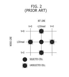
Another major obstacle is the sneak path current problem in crossbar architectures, which can lead to misreading of memory cells. While selector devices have been proposed as solutions, integrating these components without compromising the density advantage of ReRAM remains challenging. The trade-off between low operating current and stable resistance states also presents a fundamental design dilemma that researchers continue to address through material engineering and novel device structures.
Endurance limitations represent another significant barrier, particularly for applications requiring frequent write operations. Although some ReRAM cells have demonstrated endurance exceeding 10^9 cycles, this performance often comes at the expense of other parameters such as retention time or operating voltage. The underlying physical mechanisms of resistance switching, including filament formation and rupture processes, still require deeper scientific understanding to overcome these limitations.
Scaling issues also present challenges as the industry moves toward smaller technology nodes. As cell dimensions decrease, maintaining the same resistance window becomes increasingly difficult due to reduced material volumes available for filament formation. Additionally, the integration of ReRAM with standard CMOS processes introduces compatibility challenges, particularly regarding thermal budgets and material contamination concerns.
From a manufacturing perspective, yield and cost remain significant barriers. The complex materials used in ReRAM cells, often including transition metal oxides and noble metals, introduce process variability that affects production yields. Furthermore, the lack of standardized testing methodologies for ReRAM devices complicates quality assurance and reliability assessment across the industry, slowing down the path to mass production and commercialization.
Despite these advancements, ReRAM faces several critical technical barriers that have hindered its widespread commercial adoption. The most significant challenge remains the variability in resistance states, which affects both device-to-device and cycle-to-cycle performance. This inconsistency creates reliability concerns for large-scale memory arrays and complicates the design of sensing circuits required to accurately read stored data.
Another major obstacle is the sneak path current problem in crossbar architectures, which can lead to misreading of memory cells. While selector devices have been proposed as solutions, integrating these components without compromising the density advantage of ReRAM remains challenging. The trade-off between low operating current and stable resistance states also presents a fundamental design dilemma that researchers continue to address through material engineering and novel device structures.
Endurance limitations represent another significant barrier, particularly for applications requiring frequent write operations. Although some ReRAM cells have demonstrated endurance exceeding 10^9 cycles, this performance often comes at the expense of other parameters such as retention time or operating voltage. The underlying physical mechanisms of resistance switching, including filament formation and rupture processes, still require deeper scientific understanding to overcome these limitations.
Scaling issues also present challenges as the industry moves toward smaller technology nodes. As cell dimensions decrease, maintaining the same resistance window becomes increasingly difficult due to reduced material volumes available for filament formation. Additionally, the integration of ReRAM with standard CMOS processes introduces compatibility challenges, particularly regarding thermal budgets and material contamination concerns.
From a manufacturing perspective, yield and cost remain significant barriers. The complex materials used in ReRAM cells, often including transition metal oxides and noble metals, introduce process variability that affects production yields. Furthermore, the lack of standardized testing methodologies for ReRAM devices complicates quality assurance and reliability assessment across the industry, slowing down the path to mass production and commercialization.
Current ReRAM Implementation Approaches
01 Resistive RAM device structures
Resistive RAM (RRAM) devices are constructed with specific structural configurations to optimize performance. These structures typically include a resistive switching layer sandwiched between two electrodes. Various materials can be used for the resistive layer, including metal oxides, chalcogenides, and perovskites. The electrode materials and their interfaces with the resistive layer play crucial roles in determining switching characteristics. Advanced RRAM structures may incorporate additional layers for improved stability, retention, and endurance.- Resistive RAM device structures: Resistive RAM (RRAM) devices are constructed with specific structural configurations to optimize performance. These structures typically include a resistive switching layer sandwiched between two electrodes. Various materials can be used for the resistive layer, including metal oxides, chalcogenides, and perovskites. The electrode materials and their interfaces with the resistive layer play crucial roles in determining switching characteristics. Advanced RRAM structures may incorporate additional layers for improved stability, retention, and endurance.
- Resistive switching mechanisms: The operation of resistive RAM relies on various switching mechanisms that change the resistance state of the memory cell. These mechanisms include filamentary conduction, where conductive filaments form and rupture within the resistive layer, and interface-type switching, where the resistance changes at the electrode-oxide interface. Oxygen vacancy migration, ion movement, and phase changes are common physical processes underlying these switching behaviors. Understanding these mechanisms is essential for designing RRAM devices with improved reliability and performance characteristics.
- Integration and fabrication techniques: Fabrication of resistive RAM involves specialized techniques to ensure proper device operation and integration with existing semiconductor technologies. These techniques include precise deposition methods for the resistive switching layer, such as atomic layer deposition, sputtering, and sol-gel processes. Integration challenges include compatibility with CMOS processes, 3D stacking capabilities, and scaling to smaller dimensions. Advanced fabrication approaches focus on controlling material interfaces, reducing variability, and enhancing yield for mass production.
- Circuit design and operation methods: Effective operation of resistive RAM requires specialized circuit designs and operation methods. These include sensing circuits that can detect the resistance state accurately, write circuits that apply appropriate voltage pulses for switching, and addressing schemes for accessing specific memory cells. Advanced operation methods incorporate techniques to mitigate variability, reduce power consumption, and enhance endurance. Circuit designs must also address challenges such as sneak path currents in crossbar arrays and provide solutions for reliable multi-bit storage in a single cell.
- Material innovations for RRAM: Material selection and engineering are critical for resistive RAM performance. Innovative materials being explored include various metal oxides (HfOx, TaOx, TiOx), complex oxides, and two-dimensional materials. Doping strategies are employed to control defect concentrations and improve switching characteristics. Interface engineering between the electrodes and switching layer enhances stability and reduces variability. Emerging material systems aim to address challenges such as retention, endurance, and switching speed while maintaining CMOS compatibility for practical applications.
02 Resistive switching mechanisms
The operation of resistive RAM relies on various switching mechanisms that change the resistance state of the memory cell. These mechanisms include filamentary conduction, where conductive filaments form and rupture within the resistive layer, and interface-type switching, where the resistance changes at the electrode-oxide interface. Other mechanisms involve oxygen vacancy migration, ion migration, or phase change phenomena. Understanding these mechanisms is essential for designing RRAM devices with improved performance characteristics such as lower power consumption, faster switching speed, and better reliability.Expand Specific Solutions03 Manufacturing and fabrication techniques
Various manufacturing and fabrication techniques are employed to produce high-quality resistive RAM devices. These include atomic layer deposition, physical vapor deposition, chemical vapor deposition, and sputtering for thin film formation. Lithography processes are used to define device structures at nanoscale dimensions. Post-deposition treatments such as annealing and plasma treatments can optimize the resistive switching properties. Integration with CMOS technology requires specific process considerations to ensure compatibility with existing semiconductor manufacturing flows.Expand Specific Solutions04 Circuit design and memory architecture
Circuit designs for resistive RAM implementation focus on addressing, sensing, and control circuitry to effectively operate memory arrays. These designs include crossbar architectures that maximize density, selector devices to mitigate sneak path currents, and sense amplifiers to detect resistance states. Memory architectures may incorporate hierarchical bit-line and word-line structures, reference cells for reliable reading, and peripheral circuits for programming and erasing operations. Advanced designs address issues such as variability, noise margins, and power consumption to enable large-scale memory arrays.Expand Specific Solutions05 Novel materials and performance enhancement
Research on novel materials aims to enhance resistive RAM performance metrics such as endurance, retention, and switching speed. Materials under investigation include doped metal oxides, two-dimensional materials, and nanocomposites. Performance enhancement strategies include interface engineering to control ion migration, doping to modify defect concentrations, and multi-layer stacks to optimize switching behavior. These approaches address challenges such as resistance drift, variability between cells, and reliability under various operating conditions, pushing RRAM technology toward higher density and lower power applications.Expand Specific Solutions
Key Industry Players in ReRAM Development
The Resistive RAM (ReRAM) semiconductor industry is currently in a transitional growth phase, with the market expected to expand significantly as this emerging non-volatile memory technology addresses limitations of traditional flash memory. The global ReRAM market is projected to reach several billion dollars by 2028, driven by applications in IoT, AI, and edge computing. Technology maturity varies across key players: KIOXIA, Micron, and Samsung lead in commercialization efforts, while Intel, Toshiba, and CrossBar are advancing innovative architectures. Academic-industry partnerships involving Peking University, Fudan University, and IMEC are accelerating development. TSMC, GlobalFoundries, and SMIC are integrating ReRAM into their foundry processes, while IBM and Fujitsu focus on enterprise applications, positioning ReRAM as a crucial component in next-generation computing systems.
KIOXIA Corp.
Technical Solution: KIOXIA (formerly Toshiba Memory) has developed advanced ReRAM technology based on metal oxide materials, particularly focusing on tantalum oxide-based switching layers. Their approach utilizes a unique dual-layer structure combining oxygen-rich and oxygen-deficient layers to precisely control the formation and rupture of conductive filaments[1]. KIOXIA's ReRAM technology demonstrates excellent scalability down to sub-20nm nodes while maintaining reliable switching characteristics. Their devices achieve switching speeds below 50ns, endurance of over 10^6 cycles, and retention times exceeding 10 years at 85°C[2]. The company has integrated their ReRAM technology with innovative selector devices to enable high-density crossbar arrays while minimizing sneak path currents, a critical challenge for ReRAM commercialization[3]. KIOXIA has also developed specialized programming algorithms that enhance the reliability and endurance of their ReRAM cells by precisely controlling the current during set and reset operations, mitigating issues related to over-programming and variability[4]. Their manufacturing approach leverages existing semiconductor fabrication infrastructure, enabling cost-effective production and integration with logic processes.
Strengths: Strong heritage in memory technology from Toshiba; extensive manufacturing expertise and facilities; established relationships with device manufacturers. Weaknesses: Relatively recent corporate restructuring (from Toshiba Memory to KIOXIA) may have created transitional challenges; strong focus on NAND flash business may limit resources allocated to emerging ReRAM technology.
International Business Machines Corp.
Technical Solution: IBM has pioneered phase-change memory (PCM) technology, a type of resistive memory that utilizes chalcogenide glass that changes between crystalline and amorphous states. Their approach has evolved to include multi-level cell capabilities, storing 3-4 bits per cell through precise control of partial crystallization states[1]. IBM's ReRAM research has demonstrated devices with switching speeds below 10ns, endurance exceeding 10^9 cycles, and excellent data retention characteristics even at elevated temperatures[2]. The company has developed innovative drift-resistant cell designs and programming algorithms that mitigate resistance drift issues common in phase-change materials, significantly improving the long-term reliability of multi-level storage[3]. IBM has also explored the use of ReRAM for neuromorphic computing applications, leveraging the analog nature of resistive switching to implement artificial synapses for neural network hardware. Their devices demonstrate the gradual conductance changes necessary for implementing spike-timing-dependent plasticity and other learning mechanisms[4]. Additionally, IBM has developed 3D integration techniques for stacking ReRAM arrays, dramatically increasing storage density while maintaining the performance advantages of the technology[5].
Strengths: Extensive research capabilities and intellectual property portfolio; strong expertise in materials science and device physics; innovative applications beyond traditional memory storage. Weaknesses: Limited manufacturing infrastructure compared to dedicated memory producers; focus on research rather than commercialization may delay market entry; challenges in transitioning from research prototypes to mass production.
Critical Patents and Breakthroughs in ReRAM Technology
Resistive RAM, method for fabricating the same, and method for driving the same
PatentActiveUS9214631B2
Innovation
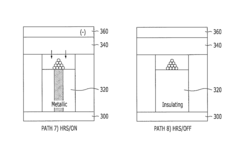
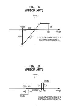
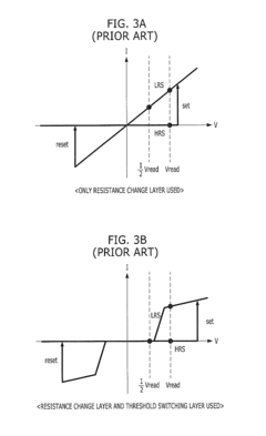
- A ReRAM is fabricated using a method where a stoichiometric transition oxide threshold switching layer and a non-stoichiometric transition metal oxide resistance change layer are formed simultaneously without sequential stacking, with the threshold switching layer comprising stoichiometric oxides like niobium or vanadium oxide, and the resistance change layer formed by oxidizing a part of the electrode, allowing for controlled resistance changes and improved read operations.
Resistive Devices and Methods of Operation Thereof
PatentActiveUS20150162079A1
Innovation
- A method of operating a resistive switching device involves applying a signal pulse with specific ramp characteristics, including a first ramp from a first voltage to a second voltage, a second ramp from the second voltage to a third voltage, and a third ramp from the third voltage to a fourth voltage, where the second and third ramps have opposite slopes, to effectively change the resistive switching device's state.


Energy Efficiency Comparison with Traditional Memory
Energy efficiency has emerged as a critical factor in the semiconductor industry's shift towards Resistive Random Access Memory (ReRAM). Traditional memory technologies such as Dynamic Random Access Memory (DRAM) and Flash memory have reached fundamental physical limitations in terms of power consumption. DRAM requires constant refreshing of its capacitors to maintain stored data, consuming significant power even in idle states. Flash memory, while non-volatile, requires high programming voltages that result in substantial energy expenditure during write operations.
ReRAM demonstrates remarkable advantages in energy efficiency metrics. During read operations, ReRAM typically consumes 10-100 times less energy compared to DRAM and Flash memory. This efficiency stems from its fundamental operating principle - data storage through resistance states rather than charge storage - eliminating the need for refresh operations that plague DRAM systems.
Write operations show even more dramatic efficiency improvements. ReRAM write energy can be as low as 0.1-1 picojoules per bit, compared to 10-100 picojoules for NAND Flash and 2-5 picojoules for DRAM. This order-of-magnitude improvement translates directly to reduced thermal management requirements and extended battery life in portable devices.
Standby power consumption represents another significant advantage for ReRAM technology. Unlike DRAM, which requires continuous refresh cycles consuming milliwatts of power, ReRAM's non-volatile nature allows for near-zero standby power. This characteristic is particularly valuable in IoT applications and energy-harvesting systems where devices may remain dormant for extended periods.
System-level energy assessments further highlight ReRAM's efficiency benefits. When integrated into computing architectures, ReRAM-based systems have demonstrated 40-60% total energy reduction compared to equivalent DRAM-based systems. This improvement stems not only from the memory cells themselves but also from reduced data movement between processing units and memory - a concept known as compute-in-memory that ReRAM naturally enables.
Thermal management requirements also favor ReRAM adoption. The technology's lower operating power translates to reduced heat generation, allowing for simpler cooling solutions and higher device density. This advantage becomes particularly important in data center environments, where cooling costs represent a substantial portion of operational expenses.
As semiconductor manufacturing processes continue to advance, the energy efficiency gap between ReRAM and traditional memory technologies is expected to widen further. ReRAM's simpler cell structure provides greater scaling potential without the corresponding increase in leakage currents that plague highly scaled DRAM and Flash technologies.
ReRAM demonstrates remarkable advantages in energy efficiency metrics. During read operations, ReRAM typically consumes 10-100 times less energy compared to DRAM and Flash memory. This efficiency stems from its fundamental operating principle - data storage through resistance states rather than charge storage - eliminating the need for refresh operations that plague DRAM systems.
Write operations show even more dramatic efficiency improvements. ReRAM write energy can be as low as 0.1-1 picojoules per bit, compared to 10-100 picojoules for NAND Flash and 2-5 picojoules for DRAM. This order-of-magnitude improvement translates directly to reduced thermal management requirements and extended battery life in portable devices.
Standby power consumption represents another significant advantage for ReRAM technology. Unlike DRAM, which requires continuous refresh cycles consuming milliwatts of power, ReRAM's non-volatile nature allows for near-zero standby power. This characteristic is particularly valuable in IoT applications and energy-harvesting systems where devices may remain dormant for extended periods.
System-level energy assessments further highlight ReRAM's efficiency benefits. When integrated into computing architectures, ReRAM-based systems have demonstrated 40-60% total energy reduction compared to equivalent DRAM-based systems. This improvement stems not only from the memory cells themselves but also from reduced data movement between processing units and memory - a concept known as compute-in-memory that ReRAM naturally enables.
Thermal management requirements also favor ReRAM adoption. The technology's lower operating power translates to reduced heat generation, allowing for simpler cooling solutions and higher device density. This advantage becomes particularly important in data center environments, where cooling costs represent a substantial portion of operational expenses.
As semiconductor manufacturing processes continue to advance, the energy efficiency gap between ReRAM and traditional memory technologies is expected to widen further. ReRAM's simpler cell structure provides greater scaling potential without the corresponding increase in leakage currents that plague highly scaled DRAM and Flash technologies.
Manufacturing Scalability and Integration Challenges
The manufacturing scalability of Resistive RAM (ReRAM) represents one of the most critical challenges in its path to widespread commercial adoption. Current semiconductor fabrication facilities are heavily optimized for traditional CMOS processes, making the integration of novel materials required for ReRAM a significant hurdle. The transition demands substantial modifications to existing manufacturing lines, with particular attention to material deposition techniques and process control parameters.
ReRAM devices typically require specialized metal oxides such as HfO₂, TiO₂, or Ta₂O₅ that must be deposited with precise stoichiometry and thickness control. The industry faces challenges in achieving consistent switching layer formation across large-diameter wafers, with variations as small as 1-2nm potentially causing significant performance differences between devices. This uniformity issue becomes increasingly problematic as manufacturers attempt to scale to advanced nodes below 28nm.
Integration with CMOS backend processes presents another major obstacle. The thermal budget constraints of CMOS backend processing (typically limited to 400-450°C) restrict the processing options for ReRAM elements. Additionally, potential material contamination concerns arise when introducing new metals into fabrication facilities, requiring careful isolation protocols and dedicated equipment in some cases.
Yield management represents a persistent challenge, with current ReRAM manufacturing yields significantly lower than those of mature memory technologies. The formation of conductive filaments—the fundamental mechanism enabling ReRAM operation—remains difficult to control precisely at scale. Statistical variations in filament formation lead to device-to-device variability that impacts reliability and performance consistency across large arrays.
3D integration approaches, while promising for density improvements, introduce additional complexities in manufacturing. Vertical stacking of ReRAM cells requires precise alignment and interconnection techniques that are still evolving. The industry is exploring various approaches including through-silicon vias (TSVs) and monolithic 3D integration, each with their own set of manufacturing challenges.
Equipment suppliers are gradually developing specialized tools for ReRAM manufacturing, but the ecosystem remains less mature compared to established memory technologies. The lack of standardized processes and equipment configurations increases production costs and slows industry-wide adoption. Leading semiconductor equipment manufacturers have begun offering dedicated solutions for ReRAM fabrication, though these often require significant customization for specific implementations.
ReRAM devices typically require specialized metal oxides such as HfO₂, TiO₂, or Ta₂O₅ that must be deposited with precise stoichiometry and thickness control. The industry faces challenges in achieving consistent switching layer formation across large-diameter wafers, with variations as small as 1-2nm potentially causing significant performance differences between devices. This uniformity issue becomes increasingly problematic as manufacturers attempt to scale to advanced nodes below 28nm.
Integration with CMOS backend processes presents another major obstacle. The thermal budget constraints of CMOS backend processing (typically limited to 400-450°C) restrict the processing options for ReRAM elements. Additionally, potential material contamination concerns arise when introducing new metals into fabrication facilities, requiring careful isolation protocols and dedicated equipment in some cases.
Yield management represents a persistent challenge, with current ReRAM manufacturing yields significantly lower than those of mature memory technologies. The formation of conductive filaments—the fundamental mechanism enabling ReRAM operation—remains difficult to control precisely at scale. Statistical variations in filament formation lead to device-to-device variability that impacts reliability and performance consistency across large arrays.
3D integration approaches, while promising for density improvements, introduce additional complexities in manufacturing. Vertical stacking of ReRAM cells requires precise alignment and interconnection techniques that are still evolving. The industry is exploring various approaches including through-silicon vias (TSVs) and monolithic 3D integration, each with their own set of manufacturing challenges.
Equipment suppliers are gradually developing specialized tools for ReRAM manufacturing, but the ecosystem remains less mature compared to established memory technologies. The lack of standardized processes and equipment configurations increases production costs and slows industry-wide adoption. Leading semiconductor equipment manufacturers have begun offering dedicated solutions for ReRAM fabrication, though these often require significant customization for specific implementations.
Unlock deeper insights with PatSnap Eureka Quick Research — get a full tech report to explore trends and direct your research. Try now!
Generate Your Research Report Instantly with AI Agent
Supercharge your innovation with PatSnap Eureka AI Agent Platform!