Trends in Chiplet Use for Artificial Intelligence Acceleration
JUL 16, 20259 MIN READ
Generate Your Research Report Instantly with AI Agent
Patsnap Eureka helps you evaluate technical feasibility & market potential.
Chiplet AI Acceleration Background and Objectives
Chiplet technology has emerged as a revolutionary approach in the semiconductor industry, particularly in the realm of artificial intelligence (AI) acceleration. This modular design paradigm allows for the integration of multiple smaller chips, or "chiplets," onto a single package, offering enhanced performance, scalability, and cost-effectiveness compared to traditional monolithic chip designs.
The evolution of chiplet technology for AI acceleration can be traced back to the increasing demands for computational power in AI applications. As AI models grew in complexity and size, traditional chip designs struggled to keep pace with the exponential growth in computational requirements. This led to the exploration of alternative architectures that could deliver higher performance while maintaining power efficiency and manufacturing feasibility.
The primary objective of chiplet-based AI acceleration is to overcome the limitations of monolithic chip designs, such as yield issues, scalability constraints, and rising manufacturing costs. By disaggregating complex system-on-chip (SoC) designs into smaller, more manageable chiplets, manufacturers can achieve better yields, reduce costs, and improve overall system performance.
Chiplet technology aligns with the trend of heterogeneous computing in AI acceleration. It enables the integration of diverse processing elements, such as CPUs, GPUs, and specialized AI accelerators, onto a single package. This heterogeneous integration allows for optimized performance across various AI workloads, from training large neural networks to inference at the edge.
The development of chiplet-based AI accelerators is driven by several key technological advancements. These include advanced packaging technologies like 2.5D and 3D integration, high-bandwidth interconnects such as silicon interposers and advanced interface standards, and sophisticated die-to-die communication protocols.
As the AI industry continues to evolve, chiplet technology is expected to play a crucial role in addressing the growing demand for more powerful and efficient AI hardware. The modular nature of chiplets allows for rapid innovation and customization, enabling AI accelerator designers to quickly adapt to new AI algorithms and workloads.
Looking ahead, the objectives for chiplet-based AI acceleration include further improvements in energy efficiency, reduction in manufacturing costs, and enhanced scalability to support increasingly complex AI models. Additionally, there is a focus on developing standardized interfaces and protocols to facilitate interoperability between chiplets from different manufacturers, potentially leading to a more diverse and competitive ecosystem in AI hardware.
Market Demand for AI Chiplet Solutions
The market demand for AI chiplet solutions has been experiencing significant growth, driven by the increasing complexity and computational requirements of artificial intelligence applications. As AI algorithms become more sophisticated and data-intensive, traditional monolithic chip designs are struggling to meet the performance, power efficiency, and cost-effectiveness demands of modern AI workloads.
Chiplet-based solutions offer a modular approach to chip design, allowing for greater flexibility and scalability in AI acceleration. This modularity enables companies to mix and match different chiplets to create customized AI solutions tailored to specific use cases, from edge devices to data centers. The ability to integrate heterogeneous components, such as high-performance compute cores, memory, and I/O interfaces, on a single package is particularly attractive for AI applications that require diverse processing capabilities.
The demand for AI chiplets is further fueled by the need for more efficient and cost-effective manufacturing processes. By leveraging advanced packaging technologies, chiplet-based designs can potentially reduce production costs and improve yields compared to large monolithic chips. This aspect is particularly crucial as AI models continue to grow in size and complexity, requiring ever-increasing computational resources.
In the data center and cloud computing sector, there is a strong demand for AI chiplets that can deliver high performance while maintaining energy efficiency. Hyperscalers and cloud service providers are actively seeking solutions that can accelerate AI training and inference tasks while minimizing power consumption and operational costs. This has led to increased interest in chiplet-based AI accelerators that can be easily integrated into existing server architectures.
The edge computing market is another key driver for AI chiplet solutions. As more AI processing moves to the edge for applications such as autonomous vehicles, smart cities, and industrial IoT, there is a growing need for compact, power-efficient AI accelerators. Chiplet-based designs offer the potential to create highly optimized edge AI solutions that balance performance, power consumption, and form factor constraints.
The automotive industry is also showing significant interest in AI chiplets for advanced driver assistance systems (ADAS) and autonomous driving technologies. The ability to create scalable and upgradable AI platforms using chiplets is particularly appealing in this sector, where rapid technological advancements and stringent safety requirements necessitate flexible and future-proof solutions.
Current State and Challenges in Chiplet-based AI Accelerators
The current state of chiplet-based AI accelerators reflects a rapidly evolving landscape in the semiconductor industry. Chiplets have emerged as a promising solution to address the challenges of traditional monolithic chip designs, particularly in the context of AI acceleration. This approach allows for the integration of multiple smaller dies onto a single package, offering improved performance, power efficiency, and cost-effectiveness.
One of the primary challenges in chiplet-based AI accelerators is the interconnect technology. As AI workloads demand increasingly higher bandwidth and lower latency, the communication between chiplets becomes a critical bottleneck. Current solutions, such as Intel's EMIB (Embedded Multi-die Interconnect Bridge) and TSMC's CoWoS (Chip on Wafer on Substrate), are pushing the boundaries of interconnect capabilities, but further advancements are needed to meet future AI acceleration requirements.
Another significant challenge is thermal management. The high-density integration of chiplets can lead to increased heat generation, potentially impacting performance and reliability. Innovative cooling solutions, including advanced packaging techniques and novel materials, are being explored to address this issue.
Standardization remains a key hurdle in the widespread adoption of chiplet-based designs. The lack of universal standards for chiplet interfaces and protocols hinders interoperability and limits the potential for mix-and-match solutions from different vendors. Initiatives like the Universal Chiplet Interconnect Express (UCIe) consortium are working towards establishing industry-wide standards, but widespread adoption is still in progress.
Manufacturing and testing complexities pose additional challenges. The assembly of multiple chiplets requires precise alignment and bonding techniques, which can impact yield and cost. Furthermore, testing chiplet-based systems is more complex than traditional monolithic designs, necessitating new approaches to ensure reliability and performance.
Despite these challenges, chiplet-based AI accelerators have shown promising results. Companies like AMD, Intel, and NVIDIA are actively developing and deploying chiplet architectures in their AI-focused products. These designs have demonstrated significant improvements in performance scaling, allowing for more powerful AI accelerators that can handle increasingly complex neural networks and machine learning models.
The current state of chiplet technology for AI acceleration is characterized by rapid innovation and ongoing research. As the industry continues to address the challenges of interconnects, thermal management, standardization, and manufacturing, chiplet-based designs are poised to play a crucial role in the future of AI hardware. The potential for customization and scalability offered by chiplets aligns well with the diverse and evolving needs of AI applications, making this approach a key focus area for semiconductor companies and AI hardware developers.
Existing Chiplet Architectures for AI Acceleration
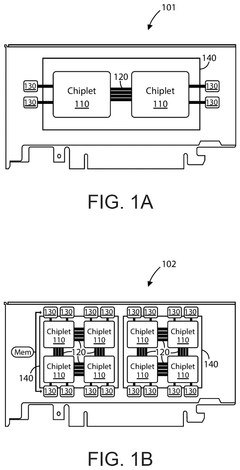
01 Chiplet integration and packaging
Chiplets are integrated circuit dies that can be combined in a single package to create more complex systems. This approach allows for modular design, improved yield, and cost-effective manufacturing of high-performance computing systems. Advanced packaging technologies are used to interconnect these chiplets, enabling high-bandwidth and low-latency communication between different functional blocks.- Chiplet integration and packaging: Chiplets are integrated circuit dies that can be combined to form larger, more complex systems. This approach allows for modular design and improved manufacturing yields. Advanced packaging techniques are used to interconnect these chiplets, enabling high-performance and cost-effective multi-chip solutions.
- Interconnect technologies for chiplets: Various interconnect technologies are employed to facilitate communication between chiplets. These may include advanced interposers, through-silicon vias (TSVs), and high-bandwidth interfaces. The choice of interconnect technology impacts the overall performance, power efficiency, and scalability of chiplet-based systems.
- Thermal management in chiplet designs: Effective thermal management is crucial in chiplet-based systems due to the high power density and potential hotspots. Innovative cooling solutions and thermal interface materials are developed to ensure optimal performance and reliability of chiplet assemblies.
- Chiplet-based AI and machine learning accelerators: Chiplets are increasingly used in the design of AI and machine learning accelerators. This modular approach allows for the integration of specialized processing units, memory, and I/O interfaces, enabling highly efficient and scalable AI computing solutions.
- Chiplet standardization and ecosystem development: Efforts are underway to standardize chiplet interfaces and protocols, fostering a more open ecosystem for chiplet-based designs. This standardization aims to improve interoperability between chiplets from different vendors and accelerate the adoption of chiplet technology across the semiconductor industry.
02 Interconnect technologies for chiplets
Various interconnect technologies are employed to facilitate communication between chiplets within a package. These may include through-silicon vias (TSVs), micro-bumps, and advanced interposers. The choice of interconnect technology impacts the overall performance, power efficiency, and thermal management of the chiplet-based system.Expand Specific Solutions03 Chiplet-based system architecture
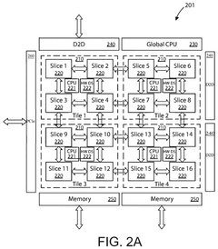
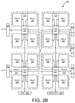
Chiplet-based systems can be designed with different architectural approaches, such as heterogeneous integration of diverse functional blocks or homogeneous arrays of identical chiplets. These architectures aim to optimize performance, power consumption, and scalability for specific application domains, including high-performance computing, artificial intelligence, and edge computing.Expand Specific Solutions04 Thermal management in chiplet designs
Effective thermal management is crucial in chiplet-based systems due to the high power density and potential hotspots. Advanced cooling solutions, such as integrated liquid cooling or novel heat spreader designs, are developed to address thermal challenges and maintain optimal performance of chiplet-based processors and systems.Expand Specific Solutions05 Testing and yield improvement for chiplets
Specialized testing methodologies and yield improvement techniques are developed for chiplet-based designs. These include pre-integration testing of individual chiplets, known-good-die strategies, and post-integration system-level testing. Advanced fault tolerance and redundancy schemes are also implemented to enhance the overall yield and reliability of chiplet-based systems.Expand Specific Solutions
Key Players in AI Chiplet Industry
The chiplet market for AI acceleration is in a dynamic growth phase, characterized by increasing market size and evolving technological maturity. Major players like Intel, Qualcomm, and Huawei are driving innovation, while emerging companies such as D-Matrix and MemryX are introducing specialized solutions. The market is seeing a shift towards more modular and efficient chip designs, with companies like Micron and SK hynix contributing to memory-centric approaches. As AI workloads become more complex, the demand for high-performance, energy-efficient chiplet solutions is expected to grow, fostering competition and collaboration among established semiconductor giants and innovative startups.
Huawei Technologies Co., Ltd.
Technical Solution: Huawei's approach to chiplet-based AI acceleration is exemplified by their Ascend AI processors. The company has developed a chiplet architecture that allows for scalable AI performance across different product lines. Huawei's Da Vinci architecture, used in their Ascend series, employs a modular design that can be adapted for various AI workloads[3]. The Ascend 910 AI processor, for instance, utilizes multiple AI cores interconnected through a high-bandwidth on-chip network, enabling efficient parallel processing for large-scale AI models[4]. Huawei has also invested in advanced packaging technologies to support their chiplet designs, including their own version of 2.5D and 3D integration techniques.
Strengths: Scalable AI performance, customization for different AI workloads, and in-house packaging technologies. Weaknesses: Geopolitical challenges affecting access to advanced manufacturing processes and global markets.
QUALCOMM, Inc.
Technical Solution: Qualcomm's approach to chiplet-based AI acceleration is integrated into their mobile and edge computing platforms. The company's Snapdragon series of SoCs incorporates AI accelerators as part of a heterogeneous computing architecture. While not traditionally using a multi-chip module approach, Qualcomm has been exploring chiplet technologies for future designs. Their AI Engine, present in recent Snapdragon platforms, utilizes a combination of CPU, GPU, and dedicated AI processing units to accelerate AI workloads[5]. Qualcomm has also been investing in advanced packaging technologies and has patents related to chiplet-based designs for mobile and IoT devices[6]. The company's focus is on energy-efficient AI acceleration for edge devices, leveraging their expertise in mobile technologies.
Strengths: Strong presence in mobile and edge computing, energy-efficient designs, and expertise in heterogeneous computing. Weaknesses: Less experience with large-scale AI accelerators compared to data center-focused competitors.
Core Innovations in Chiplet-based AI Hardware
Server system using switch linking for communication between ai accelerator apparatuses with in-memory compute chiplet devices
PatentPendingUS20250061319A1
Innovation
- The development of AI accelerator apparatuses and chiplet devices with in-memory compute (IMC) capabilities, which include digital IMC (DIMC) devices for matrix computations and SIMD devices for non-matrix computations, along with a modular architecture that allows for scalable and efficient processing of transformer workloads.


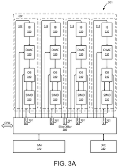
Ai accelerator apparatus using in-memory compute chiplet devices for transformer workloads
PatentPendingUS20250036582A1
Innovation
- The development of AI accelerator apparatuses using in-memory compute chiplet devices, which include digital in-memory compute (DIMC) devices and single input multiple data (SIMD) devices, to accelerate transformer computations by integrating computational functions and memory fabric.

Thermal Management in AI Chiplet Systems
Thermal management has become a critical challenge in AI chiplet systems as the demand for higher performance and increased integration continues to grow. The use of chiplets in AI acceleration has led to more compact and powerful designs, but it has also intensified the heat dissipation issues. As chiplets are packed closer together, the power density increases, resulting in localized hotspots and overall higher thermal loads.
To address these challenges, various thermal management techniques have been developed and implemented in AI chiplet systems. One of the primary approaches is the use of advanced cooling solutions, such as liquid cooling and immersion cooling. These methods offer superior heat dissipation capabilities compared to traditional air cooling, allowing for higher power densities and improved performance.
Another key strategy in thermal management is the optimization of chiplet placement and interconnect design. By carefully arranging chiplets and considering thermal characteristics during the design phase, engineers can minimize hotspots and improve overall heat distribution. This approach often involves the use of thermal simulation tools to predict and optimize thermal performance before physical implementation.
Advanced packaging technologies also play a crucial role in thermal management for AI chiplet systems. The development of 2.5D and 3D packaging techniques has enabled better thermal interfaces between chiplets and heat spreaders, improving overall heat dissipation. Additionally, the use of through-silicon vias (TSVs) and interposers can facilitate more efficient heat transfer pathways.
Dynamic thermal management techniques have gained prominence in AI chiplet systems. These methods involve real-time monitoring of temperature and power consumption, allowing for adaptive control of clock speeds, voltage levels, and workload distribution. By dynamically adjusting these parameters, the system can maintain optimal performance while preventing thermal throttling or damage.
The integration of on-chip thermal sensors and dedicated thermal management units has become increasingly common in AI chiplet designs. These components provide accurate temperature data and enable fine-grained control over thermal characteristics, allowing for more sophisticated and responsive thermal management strategies.
As AI chiplet systems continue to evolve, research into novel materials and cooling technologies is ongoing. This includes the exploration of phase-change materials, graphene-based heat spreaders, and microfluidic cooling channels integrated directly into the chiplet package. These innovations aim to push the boundaries of thermal management, enabling even higher performance and integration levels in future AI acceleration systems.
Standardization Efforts in AI Chiplet Ecosystem
Standardization efforts in the AI chiplet ecosystem are gaining momentum as the industry recognizes the need for interoperability and compatibility among different chiplet designs. The development of common interfaces and protocols is crucial for enabling seamless integration of diverse AI accelerator chiplets from various manufacturers. Several industry consortia and standards organizations are actively working on establishing frameworks and specifications to facilitate the adoption of chiplet-based AI acceleration solutions.
One of the key initiatives in this space is the Universal Chiplet Interconnect Express (UCIe) consortium, which aims to create an open industry standard for die-to-die interconnects. UCIe focuses on defining a common physical layer, protocol stack, and software model to enable chiplets from different vendors to work together efficiently. This standardization effort is particularly relevant for AI acceleration, as it allows for the integration of specialized AI processing units with other components in a modular and scalable manner.
Another significant standardization effort is the Open Compute Project's (OCP) Chiplet Design Exchange (CDX) working group. CDX is developing a set of specifications and guidelines for chiplet-based system design, with a focus on AI and high-performance computing applications. The group is working on standardizing chiplet interfaces, power delivery, and thermal management to facilitate the creation of heterogeneous AI systems using chiplets from multiple sources.
The CHIPS Alliance, an open-source hardware initiative, is also contributing to the standardization of chiplet technologies for AI acceleration. Their efforts include developing open-source tools and IP blocks that support chiplet-based design methodologies, as well as promoting interoperability standards for chiplet integration.
In addition to these industry-led initiatives, government agencies and research institutions are also playing a role in driving standardization efforts. For example, the Defense Advanced Research Projects Agency (DARPA) has launched the Common Heterogeneous Integration and IP Reuse Strategies (CHIPS) program, which aims to develop standards and design methodologies for modular chip designs, including those used in AI acceleration.
As these standardization efforts progress, they are expected to accelerate the adoption of chiplet-based architectures in AI acceleration systems. The establishment of common standards will enable greater flexibility in system design, reduce development costs, and foster innovation by allowing companies to focus on their core competencies while leveraging standardized interfaces for integration. This collaborative approach to standardization is crucial for addressing the increasing complexity and performance demands of AI workloads in a scalable and efficient manner.
Unlock deeper insights with Patsnap Eureka Quick Research — get a full tech report to explore trends and direct your research. Try now!
Generate Your Research Report Instantly with AI Agent
Supercharge your innovation with Patsnap Eureka AI Agent Platform!