UCIe Chiplet Interconnect EDA Flow And DRC Checklist
SEP 1, 20259 MIN READ
Generate Your Research Report Instantly with AI Agent
PatSnap Eureka helps you evaluate technical feasibility & market potential.
UCIe Chiplet Technology Background and Objectives
Universal Chiplet Interconnect Express (UCIe) represents a significant advancement in semiconductor integration technology, emerging as a response to the increasing challenges of traditional monolithic chip scaling. The evolution of semiconductor technology has historically followed Moore's Law, but as process nodes shrink below 5nm, the industry faces diminishing returns in performance, power efficiency, and cost benefits from traditional scaling approaches. This technological inflection point has catalyzed the development of chiplet-based architectures, where multiple smaller dies (chiplets) are integrated into a single package.
UCIe was formally introduced in March 2022 by an industry consortium including Intel, AMD, Arm, TSMC, Samsung, and other major semiconductor companies. The technology aims to establish an open, standardized interconnect specification for die-to-die communication within a package. This standardization represents a paradigm shift from proprietary interconnect solutions that previously dominated the market, such as Intel's EMIB, AMD's Infinity Fabric, and TSMC's CoWoS.
The primary objective of UCIe is to enable a disaggregated, modular approach to chip design where different functional blocks can be manufactured using optimal process nodes and then integrated into a cohesive system. This approach promises significant advantages in terms of yield improvement, design flexibility, time-to-market acceleration, and cost optimization compared to monolithic designs.
UCIe technology encompasses both physical and protocol layers. The physical layer defines the bump pitch, signal integrity requirements, and power delivery specifications, while the protocol layer addresses data formatting, flow control, and error handling mechanisms. The standard supports two primary modes: a die-to-die (D2D) mode for ultra-high-bandwidth, low-latency connections between adjacent dies, and a package-to-package (P2P) mode for longer-range connections.
The development of UCIe is driven by several market forces, including the need for specialized computing architectures for AI/ML workloads, high-performance computing demands, and edge computing requirements. These applications necessitate heterogeneous integration of various components such as CPUs, GPUs, memory, and specialized accelerators.
From an Electronic Design Automation (EDA) perspective, UCIe presents unique challenges and opportunities. The interconnect requires specialized design tools for signal integrity analysis, power integrity verification, thermal management, and physical verification including Design Rule Checking (DRC). The establishment of standardized EDA flows and DRC checklists for UCIe implementations is crucial for the technology's widespread adoption and successful implementation across the semiconductor ecosystem.
Market Demand Analysis for Chiplet-Based Solutions
The chiplet market is experiencing unprecedented growth, driven by the increasing complexity of semiconductor designs and the limitations of traditional monolithic approaches. As Moore's Law faces physical and economic constraints, chiplet-based architectures have emerged as a compelling alternative, allowing for the integration of multiple silicon dies in a single package. Market research indicates that the global chiplet market is projected to grow significantly over the next decade, with particularly strong demand in data centers, high-performance computing, and artificial intelligence applications.
The Universal Chiplet Interconnect Express (UCIe) standard has catalyzed market interest by addressing a critical industry need for standardized die-to-die interconnects. This standardization is expected to expand the chiplet ecosystem dramatically, with market analysts predicting that chiplet-based designs will represent a substantial portion of high-performance computing solutions by 2025.
From an industry perspective, several factors are driving demand for chiplet-based solutions. First, performance requirements continue to escalate across computing sectors, particularly in AI training and inference, where computational demands double approximately every 3-4 months. Traditional monolithic designs cannot scale efficiently to meet these requirements, creating a market gap that chiplet architectures can fill.
Cost considerations also play a significant role in market demand. As process nodes advance to 5nm and below, manufacturing costs increase exponentially. Chiplet approaches allow companies to optimize different components on appropriate process nodes, potentially reducing overall production costs while maintaining performance advantages. This economic benefit is particularly attractive to mid-sized semiconductor companies that cannot afford leading-edge process development for entire systems.
Supply chain resilience represents another market driver. The semiconductor industry has experienced significant disruptions in recent years, highlighting vulnerabilities in global supply chains. Chiplet-based designs offer greater flexibility in sourcing components from multiple suppliers, reducing dependency on single vendors or fabrication facilities.
The EDA tool market specifically shows strong growth potential, as existing design flows require significant adaptation to support chiplet-based architectures. Current tools lack comprehensive support for die-to-die interfaces, physical verification of chiplet boundaries, and system-level optimization across multiple dies. This gap creates substantial market opportunities for EDA vendors who can deliver integrated solutions supporting UCIe standards and associated design rule checks.
Customer surveys indicate that engineering teams are actively seeking tools that can streamline the chiplet design process, with particular emphasis on verification and validation capabilities. The complexity of ensuring signal integrity across die boundaries, managing thermal considerations, and optimizing power delivery networks represents significant challenges that customers are willing to pay premium prices to address.
UCIe Technical Challenges and Implementation Status
UCIe (Universal Chiplet Interconnect Express) represents a significant advancement in chiplet-based design methodology, yet its implementation faces several technical challenges. The current state of UCIe implementation reveals a complex landscape of both opportunities and obstacles that must be addressed for widespread adoption.
The primary technical challenge lies in the physical implementation of die-to-die interfaces that must operate at extremely high speeds (up to 32 GT/s) while maintaining signal integrity. Current EDA tools struggle to accurately model the complex electromagnetic interactions at these interfaces, particularly when dealing with the ultra-fine bump pitches (down to 25-45μm) required by UCIe specifications.
Power management presents another significant hurdle, as the high-speed SerDes components in UCIe consume substantial power. Current implementations show power efficiency ranging from 0.5 to 1 pJ/bit, which remains higher than desired for many applications. This challenge is compounded by thermal management issues that arise when multiple chiplets are placed in close proximity.
Testing methodologies for UCIe implementations remain immature. The industry lacks standardized test patterns and validation procedures specific to chiplet interfaces, making quality assurance difficult. Current implementations rely heavily on custom testing solutions, which increases development costs and time-to-market.
From a manufacturing perspective, yield management across multiple chiplets presents unique challenges. The current state shows that even with Known Good Die (KGD) testing, system-level failures can occur due to interface mismatches or signal integrity issues that only manifest when chiplets are assembled together.
The EDA flow for UCIe implementation currently requires significant manual intervention, particularly in areas of bump planning, signal routing, and power distribution. Tools from major EDA vendors have begun incorporating UCIe-specific design rule checks, but comprehensive automation remains limited.
Interoperability between chiplets from different vendors—a key promise of the UCIe standard—has seen limited real-world validation. Current implementations primarily focus on intra-company chiplet integration rather than the open ecosystem envisioned by the standard.
The DRC (Design Rule Check) landscape for UCIe is still evolving, with no universally accepted checklist. Current implementations typically rely on company-specific design rules supplemented by basic UCIe compliance checks. This fragmentation hampers the development of a truly open chiplet ecosystem.
Despite these challenges, several successful implementations have emerged, particularly in high-performance computing and data center applications. These early adopters have developed workarounds for the current limitations, often through close collaboration between design teams, EDA vendors, and foundries.
Current UCIe EDA Design Flow Solutions
01 UCIe chiplet interconnect design verification and DRC
Design Rule Checking (DRC) for UCIe chiplet interconnects involves verification of physical layout constraints to ensure manufacturability and reliability. This includes checking bump pitch, trace width, spacing requirements, and alignment tolerances specific to chiplet interfaces. Advanced EDA tools implement specialized rule decks for UCIe compliance, verifying both physical and electrical parameters to ensure proper signal integrity across die-to-die interfaces.- UCIe Chiplet Design and Verification Flow: The Universal Chiplet Interconnect Express (UCIe) design flow involves specialized EDA tools for chiplet-based system design. This includes verification methodologies to ensure proper interconnect functionality between chiplets, signal integrity analysis, and power integrity verification. The flow encompasses pre-layout simulation, post-layout verification, and comprehensive testing strategies to validate UCIe compliance before manufacturing.
- DRC Checklist for UCIe Implementation: Design Rule Check (DRC) checklists for UCIe implementations include specific requirements for die-to-die interfaces, bump pitch constraints, and physical layout rules. These checklists ensure proper spacing, width, and alignment of interconnect traces, verification of bump arrays, and adherence to UCIe specification requirements. DRC checks are critical for ensuring manufacturability and reliability of chiplet-based designs.
- Advanced Packaging and Integration for Chiplets: Advanced packaging technologies for UCIe chiplet integration include substrate design considerations, thermal management solutions, and assembly process requirements. This involves specific design rules for interposer-based integration, silicon bridge technologies, and embedded interconnects. The packaging approach must address signal integrity challenges across die boundaries while maintaining high bandwidth and low latency connections.
- EDA Tool Integration for UCIe Workflows: Electronic Design Automation (EDA) tools for UCIe workflows require specialized integration capabilities to handle multi-die designs. This includes tools for co-design and co-verification across chiplet boundaries, automated DRC checking specific to UCIe requirements, and physical verification tools that understand chiplet interfaces. The integrated toolchain must support both die-level and system-level verification to ensure proper functionality of the complete chiplet-based system.
- UCIe Protocol Compliance and Testing: UCIe protocol compliance testing involves verification of electrical and logical specifications, including signal integrity, timing requirements, and protocol adherence. This requires specialized test methodologies for die-to-die interfaces, automated compliance checking tools, and comprehensive test patterns. The testing framework must validate both physical layer and protocol layer aspects of the UCIe standard to ensure interoperability between chiplets from different vendors.
02 EDA flow optimization for chiplet-based designs
The EDA flow for UCIe chiplet designs requires specialized tools that can handle multi-die integration challenges. This includes partitioning logic across multiple chiplets, optimizing interconnect placement, and ensuring timing closure across die boundaries. The flow typically incorporates floor planning, power analysis, thermal simulation, and signal integrity verification specific to high-speed die-to-die interfaces, with automated checks to validate UCIe protocol compliance throughout the design process.Expand Specific Solutions03 Physical implementation and validation of UCIe interfaces
Physical implementation of UCIe interfaces requires precise placement and routing of high-speed interconnects between chiplets. The validation process includes checking bump arrays, microbump alignment, and ensuring proper physical dimensions according to the UCIe specification. EDA tools provide specialized capabilities for bump planning, escape routing, and signal integrity analysis to meet the stringent requirements of high-bandwidth die-to-die connections while maintaining manufacturability.Expand Specific Solutions04 Power and thermal analysis for chiplet designs
Power and thermal analysis are critical aspects of the UCIe chiplet design flow. EDA tools provide specialized capabilities to analyze power distribution networks across chiplet boundaries, identify potential hotspots, and ensure adequate thermal management. The DRC checklist includes verification of power integrity, checking for voltage drop across die-to-die interfaces, and ensuring that thermal constraints are met for the entire package, which is essential for reliable operation of high-performance chiplet-based systems.Expand Specific Solutions05 Interoperability and standardization in UCIe implementation
Ensuring interoperability between chiplets from different vendors requires strict adherence to UCIe standards. EDA flows incorporate standardized verification methods to check compliance with the UCIe specification, including protocol verification, electrical parameter validation, and physical implementation rules. The DRC checklist includes verification of standard-compliant PHY implementation, checking for proper implementation of UCIe protocol layers, and ensuring that all chiplets can communicate effectively when integrated into a single package.Expand Specific Solutions
Key Industry Players in UCIe Ecosystem
The UCIe Chiplet Interconnect EDA Flow and DRC Checklist technology landscape is currently in an early growth phase, with market size expanding rapidly as chiplet-based designs become essential for advanced computing solutions. The technology maturity is evolving, with key players driving standardization and implementation. Intel leads as a founding member of the UCIe consortium, while TSMC, Samsung, and GLOBALFOUNDRIES provide critical foundry support. EDA leaders Synopsys and Cadence are developing specialized tools for chiplet design verification. Qualcomm, Apple, AMD (formerly Xilinx), and Huawei are actively implementing chiplet architectures in their products, while SiFive contributes RISC-V expertise to the ecosystem. This collaborative yet competitive environment is accelerating the technology's adoption across high-performance computing, AI, and data center applications.
Huawei Technologies Co., Ltd.
Technical Solution: Huawei has developed a proprietary UCIe Chiplet Interconnect EDA Flow as part of their broader heterogeneous integration strategy. Their approach focuses on optimizing chiplet-based designs for high-performance computing and telecommunications applications. Huawei's EDA flow incorporates their Da Vinci architecture principles, which emphasize flexibility in connecting different types of computing elements through standardized interfaces. For UCIe implementation, Huawei has developed specialized design methodologies that address the unique challenges of high-bandwidth, low-latency die-to-die communication. Their flow includes custom tools for chiplet floorplanning that optimize the placement of UCIe interfaces to minimize latency and power consumption. Huawei's DRC checklist for UCIe compliance includes verification of signal integrity across die boundaries, thermal analysis of hotspots at interface regions, and mechanical stress analysis for the microbump arrays[7]. Their approach also incorporates advanced simulation capabilities that model both electrical and thermal interactions between chiplets in a multi-die package. Huawei has invested in developing UCIe-compliant PHY IP that can be integrated into their custom silicon designs.
Strengths: Huawei's vertical integration from chip design to system deployment allows them to optimize their UCIe implementation for specific application requirements. Their experience in telecommunications systems gives them particular insight into high-speed serial interface design. Weaknesses: Their EDA flow may be less accessible to third-party designers compared to commercial EDA vendors. The proprietary nature of some aspects of their methodology may limit interoperability with industry-standard tools and flows.
Intel Corp.
Technical Solution: Intel has pioneered UCIe (Universal Chiplet Interconnect Express) technology as a founding member of the UCIe consortium. Their approach to UCIe Chiplet Interconnect EDA Flow involves a comprehensive design methodology that integrates their Embedded Multi-die Interconnect Bridge (EMIB) technology with UCIe standards. Intel's EDA flow for UCIe implementation includes specialized tools for die-to-die interface design, signal integrity analysis, and power distribution network optimization. Their methodology encompasses pre-silicon validation through advanced simulation environments that model the electrical and thermal characteristics of chiplet interconnects. Intel has developed specific DRC (Design Rule Check) guidelines that address UCIe-specific requirements including bump pitch constraints, alignment tolerances, and signal routing rules between chiplets[1]. Their EDA flow supports both package-level and die-level verification to ensure compliance with UCIe specifications across different process nodes and packaging technologies[2].
Strengths: Intel's extensive experience in advanced packaging gives them significant advantages in UCIe implementation. Their established ecosystem of tools and IP blocks specifically designed for chiplet integration provides a mature platform for developers. Weaknesses: Their EDA flow may be optimized primarily for Intel's own manufacturing processes and packaging technologies, potentially limiting flexibility when working with third-party foundries or packaging solutions.
Critical UCIe DRC Requirements and Verification Methods
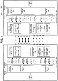
Interface conversion circuitry for universal chiplet interconnect express (UCIe)
PatentActiveUS12248419B1
Innovation
- The implementation of a converter circuit between the UCIe interface circuit and the bump interface, which includes local clock circuitry, oversampling circuitry, and majority detection circuitry, reduces the number of sideband links and corresponding bumps, thereby enhancing bandwidth density and reducing costs.
Using machine-trained network to perform DRC check
PatentWO2023141080A1
Innovation
- A machine-trained neural network, specifically a convolutional neural network, is used for pixel-based DRC checks, trained on data from traditional geometric, equation-based, and circle-tracing methods to accurately and efficiently identify design rule violations in rectilinear and curvilinear designs, leveraging deep learning and parallel processing architectures.


Interoperability and Standardization Efforts
The UCIe (Universal Chiplet Interconnect Express) consortium has made significant strides in establishing industry-wide standards for chiplet interconnection. This standardization effort represents a pivotal shift from proprietary solutions toward open ecosystems that enable multi-vendor chiplet integration. The consortium, founded by industry leaders including Intel, AMD, Arm, TSMC, and Samsung, has successfully developed specifications that address physical layer, protocol layer, and software stack requirements for chiplet-to-chiplet communication.
Interoperability testing frameworks have emerged as critical components in the UCIe ecosystem. These frameworks provide standardized methodologies for validating compliance across different vendors' chiplets. The UCIe Compliance Program, launched in 2022, offers certification processes that ensure chiplets from various manufacturers can seamlessly communicate when integrated into a single package. This program includes reference designs, test vectors, and validation suites that have been collectively developed by consortium members.
The standardization efforts extend beyond electrical specifications to encompass thermal management, mechanical form factors, and signal integrity requirements. The UCIe 1.1 specification, released in 2023, introduced enhanced power management features and expanded bandwidth options that address the growing demands of AI and high-performance computing applications. These standardized approaches to thermal and power challenges have accelerated adoption across the semiconductor industry.
EDA tool vendors have responded to UCIe standardization by developing specialized design verification and validation tools. Companies like Synopsys, Cadence, and Siemens EDA have introduced UCIe-compliant design rule checking (DRC) capabilities that automatically verify adherence to the specification. These tools implement standardized rule decks that ensure consistent interpretation of the UCIe requirements across different design environments.
Cross-industry collaboration has been particularly evident in the development of standardized testing methodologies. The Joint Electron Device Engineering Council (JEDEC) has worked alongside the UCIe consortium to align memory interface standards with chiplet interconnect requirements. Similarly, the Open Compute Project (OCP) has incorporated UCIe specifications into their next-generation server design guidelines, further cementing the standard's position in data center applications.
Future standardization roadmaps indicate expansion into advanced packaging technologies, with particular focus on heterogeneous integration challenges. The consortium is actively developing specifications for die-to-die bridges, interposers, and advanced substrate technologies that will enable more complex chiplet architectures. These efforts aim to create a comprehensive ecosystem where chiplets from different process nodes, manufacturers, and even different semiconductor materials can be seamlessly integrated.
Thermal Management Considerations for UCIe Designs
Thermal management has emerged as a critical consideration in UCIe (Universal Chiplet Interconnect Express) designs due to the increasing power densities and thermal challenges associated with chiplet integration. As chiplets are packed more densely within a package, heat dissipation becomes a significant limiting factor for system performance and reliability. The thermal design power (TDP) of UCIe implementations must be carefully managed to prevent thermal throttling and ensure consistent operation.
The thermal characteristics of UCIe interfaces present unique challenges compared to traditional monolithic designs. The die-to-die (D2D) interconnects in UCIe can create thermal hotspots at connection points, particularly in high-bandwidth configurations where signal integrity requirements drive higher power consumption. These hotspots can lead to localized temperature gradients that affect both performance and long-term reliability of the interconnect.
Current UCIe specifications define thermal parameters that must be considered during the design phase. These include maximum junction temperatures, thermal resistance requirements, and power delivery specifications across the interconnect. EDA tools must incorporate these thermal constraints into their design rule checks (DRC) to validate that implementations will operate within safe thermal envelopes under various workload scenarios.
Thermal simulation has become an essential component of the UCIe design flow. Advanced computational fluid dynamics (CFD) models are being integrated with electrical simulations to provide comprehensive electrothermal analysis. These simulations must account for the complex thermal interactions between multiple chiplets, the interposer, package substrate, and cooling solutions to accurately predict thermal behavior.
Cooling solutions for UCIe designs require special consideration due to the heterogeneous nature of chiplet-based systems. Traditional approaches such as heat spreaders and heat sinks may need modification to address the non-uniform heat distribution characteristic of multi-chiplet designs. Advanced cooling technologies including integrated liquid cooling channels, phase-change materials, and microchannel cold plates are being explored specifically for high-performance UCIe implementations.
The DRC checklist for thermal management in UCIe designs must include verification of thermal vias placement, thermal interface material (TIM) specifications, and heat spreading structures. Additionally, the checklist should verify compliance with maximum temperature gradient specifications between adjacent chiplets to prevent mechanical stress from thermal expansion mismatches, which could compromise the integrity of the interconnect.
Future UCIe specifications are expected to incorporate more sophisticated thermal management requirements as chiplet integration densities increase. This may include dynamic thermal management protocols that allow for coordinated power management across chiplets from different vendors, representing a significant advancement in heterogeneous integration capabilities.
Unlock deeper insights with PatSnap Eureka Quick Research — get a full tech report to explore trends and direct your research. Try now!
Generate Your Research Report Instantly with AI Agent
Supercharge your innovation with PatSnap Eureka AI Agent Platform!