Understanding Chiplet Impact on Semiconductor Manufacturing
JUL 16, 20259 MIN READ
Generate Your Research Report Instantly with AI Agent
Patsnap Eureka helps you evaluate technical feasibility & market potential.
Chiplet Technology Evolution and Objectives
Chiplet technology represents a paradigm shift in semiconductor manufacturing, offering a solution to the challenges posed by Moore's Law. This approach involves breaking down complex system-on-chip (SoC) designs into smaller, more manageable components called chiplets. The evolution of chiplet technology can be traced back to the early 2010s when the semiconductor industry began exploring alternatives to monolithic chip designs.
The primary objective of chiplet technology is to overcome the limitations of traditional semiconductor manufacturing processes. As transistor sizes approach atomic scales, it becomes increasingly difficult and expensive to produce large, monolithic chips with acceptable yields. Chiplets address this issue by allowing manufacturers to produce smaller, less complex dies that can be integrated into a single package.
Over the past decade, chiplet technology has progressed significantly. Initially, the focus was on developing methods for interconnecting multiple dies within a package. This led to the creation of advanced packaging technologies such as 2.5D and 3D integration. As the technology matured, industry standards emerged, facilitating interoperability between chiplets from different manufacturers.
One of the key milestones in chiplet evolution was the development of high-bandwidth, low-latency interconnect technologies. These advancements enabled chiplets to communicate efficiently, minimizing performance penalties associated with multi-die designs. Examples include AMD's Infinity Fabric and Intel's Advanced Interface Bus (AIB).
The objectives of chiplet technology extend beyond overcoming manufacturing limitations. They include improving performance, reducing power consumption, and enhancing flexibility in chip design. By allowing different components to be manufactured using optimal process nodes, chiplets enable better overall system performance and efficiency.
Looking forward, the goals of chiplet technology include further standardization of interfaces and protocols to create a more robust ecosystem. This would allow for greater mix-and-match capabilities, enabling system designers to select the best chiplets for their specific applications regardless of the manufacturer.
Another important objective is to continue improving the integration density and performance of chiplet-based systems. This involves developing more advanced packaging technologies, such as wafer-level fan-out and active interposers, which can support higher bandwidth and more complex interconnections between chiplets.
As the semiconductor industry continues to evolve, chiplet technology aims to provide a sustainable path for scaling and innovation. By enabling more modular and flexible chip designs, it has the potential to revolutionize not only semiconductor manufacturing but also the entire electronics industry, paving the way for more powerful and efficient computing systems in the future.
Market Demand for Chiplet-based Solutions
The market demand for chiplet-based solutions has been steadily growing in recent years, driven by the increasing complexity and performance requirements of modern semiconductor devices. As traditional monolithic chip designs approach their physical limits, chiplets offer a promising alternative that allows for more flexible and cost-effective manufacturing processes.
The semiconductor industry has witnessed a significant shift towards chiplet technology, particularly in high-performance computing, data centers, and artificial intelligence applications. Major players in the market, such as AMD, Intel, and TSMC, have already embraced chiplet-based designs for their advanced processors and systems-on-chip (SoCs). This adoption by industry leaders has further fueled market demand and accelerated the development of chiplet ecosystems.
One of the key drivers for chiplet-based solutions is the need for improved yield and cost-effectiveness in semiconductor manufacturing. By breaking down complex designs into smaller, more manageable components, chiplets allow manufacturers to achieve higher yields and reduce overall production costs. This approach is particularly beneficial for cutting-edge process nodes, where defect rates can be higher and manufacturing costs more substantial.
The market demand for chiplets is also influenced by the growing trend towards heterogeneous integration. As different components of a system require varying levels of performance and functionality, chiplets enable the combination of diverse technologies and process nodes within a single package. This flexibility allows for optimized performance, power efficiency, and cost-effectiveness across different parts of the system.
Furthermore, the rise of edge computing and Internet of Things (IoT) devices has created new opportunities for chiplet-based solutions. These applications often require specialized, low-power components that can be efficiently designed and manufactured using chiplet technology. The ability to mix and match different chiplets allows for rapid customization and adaptation to specific market needs, driving demand across various industry sectors.
The automotive industry has also shown increasing interest in chiplet-based solutions, particularly for advanced driver assistance systems (ADAS) and autonomous vehicles. These applications require high-performance, low-power, and highly reliable semiconductor components, which can be effectively addressed through chiplet technology.
As the market demand for chiplet-based solutions continues to grow, there is an increasing need for standardization and interoperability between different chiplet designs and manufacturers. Industry consortia and standardization efforts, such as the Universal Chiplet Interconnect Express (UCIe), are working towards establishing common interfaces and protocols to facilitate broader adoption and ecosystem development.
Chiplet Manufacturing Challenges and Limitations
While chiplets offer numerous advantages in semiconductor manufacturing, they also present significant challenges and limitations that need to be addressed. One of the primary challenges is the complexity of integration. Chiplets require precise alignment and interconnection, which demands advanced packaging technologies and sophisticated assembly processes. This increased complexity can lead to higher manufacturing costs and potential yield issues, especially in the early stages of adoption.
Another critical challenge is the need for standardization. The chiplet ecosystem requires a high degree of interoperability between components from different manufacturers. Without established industry standards for interfaces, protocols, and packaging, the widespread adoption of chiplets could be hindered. This lack of standardization also complicates supply chain management and increases the risk of compatibility issues.
Thermal management presents a unique set of challenges in chiplet-based designs. The dense integration of multiple chiplets can create hotspots and uneven heat distribution, potentially affecting performance and reliability. Innovative cooling solutions and thermal design considerations are necessary to mitigate these issues, adding another layer of complexity to the manufacturing process.
The increased number of interconnects in chiplet-based designs also raises concerns about signal integrity and power delivery. As the number of connections between chiplets grows, maintaining signal quality and ensuring efficient power distribution become more challenging. This can impact overall system performance and reliability, requiring advanced design techniques and materials to overcome these limitations.
Testing and quality assurance pose additional challenges in chiplet manufacturing. Traditional testing methods may not be sufficient for chiplet-based systems, as each chiplet needs to be tested individually and as part of the integrated system. This multi-level testing approach can increase manufacturing time and costs, potentially offsetting some of the economic benefits of chiplet technology.
Lastly, the chiplet approach introduces new considerations for intellectual property (IP) management and protection. As different chiplets may come from various suppliers, ensuring the security and integrity of proprietary designs becomes more complex. This challenge extends to the entire supply chain, requiring new strategies for IP protection and trust in multi-vendor ecosystems.
Despite these challenges, ongoing research and development efforts are focused on addressing these limitations. Advancements in packaging technologies, standardization initiatives, and innovative design approaches are continuously improving the viability and efficiency of chiplet-based semiconductor manufacturing.
Current Chiplet Integration Methodologies
01 Chiplet architecture and integration
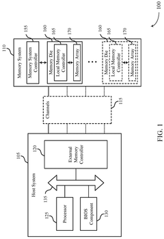
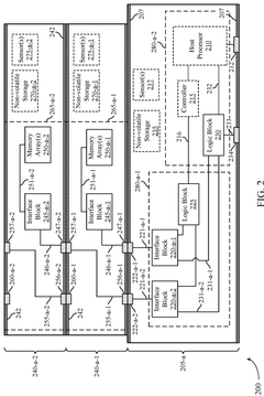
Chiplets are modular components that can be integrated to form larger, more complex systems-on-chip. This approach allows for flexible design, improved yield, and cost-effective manufacturing. The architecture involves connecting multiple smaller dies or chiplets using advanced packaging technologies, enabling the creation of high-performance, customizable semiconductor solutions.- Chiplet architecture and integration: Chiplets are modular components that can be integrated to form larger, more complex systems-on-chip. This approach allows for flexible design, improved yield, and cost-effective manufacturing. The integration of chiplets often involves advanced packaging technologies and interconnect solutions to ensure high-performance communication between different chiplet modules.
- Chiplet-based memory systems: Chiplet technology is applied to memory systems to enhance capacity, bandwidth, and energy efficiency. This approach involves designing memory chiplets that can be stacked or arranged in various configurations to meet specific performance requirements. Advanced interconnect technologies are used to ensure high-speed communication between memory chiplets and processing units.
- Power management in chiplet-based systems: Efficient power management is crucial in chiplet-based systems to optimize performance and reduce energy consumption. This involves developing sophisticated power distribution networks, implementing dynamic voltage and frequency scaling techniques, and designing power-aware interconnects between chiplets. Advanced packaging technologies also play a role in thermal management of chiplet systems.
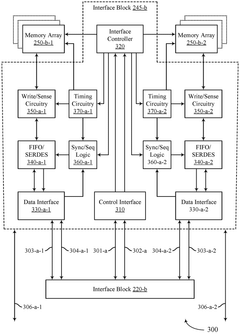
- Chiplet interconnect technologies: Developing high-speed, low-latency interconnect technologies is essential for chiplet-based systems. This includes advanced packaging solutions, such as 2.5D and 3D integration, as well as novel interconnect architectures like silicon interposers and through-silicon vias (TSVs). These technologies enable efficient communication between chiplets and help overcome bandwidth limitations in complex multi-chiplet designs.
- Chiplet design and verification methodologies: Creating effective design and verification methodologies for chiplet-based systems is crucial for ensuring reliability and performance. This involves developing new EDA tools and workflows that can handle the complexity of multi-chiplet designs, including interface standardization, system-level simulation, and design-for-test strategies. These methodologies also address challenges in chiplet reusability and integration of heterogeneous components.
02 Interconnect technologies for chiplets
Various interconnect technologies are employed to facilitate communication between chiplets and ensure high-speed data transfer. These may include advanced packaging techniques, through-silicon vias (TSVs), interposers, and high-bandwidth memory interfaces. The choice of interconnect technology impacts the overall performance, power efficiency, and thermal management of the chiplet-based system.Expand Specific Solutions03 Power management in chiplet designs
Efficient power management is crucial in chiplet-based systems to optimize performance and reduce energy consumption. This involves implementing advanced power gating techniques, dynamic voltage and frequency scaling, and intelligent power distribution across different chiplets. Thermal management strategies are also essential to maintain optimal operating conditions for each chiplet within the system.Expand Specific Solutions04 Testing and validation of chiplet-based systems
Developing effective testing and validation methodologies for chiplet-based systems is essential to ensure reliability and performance. This includes pre-silicon verification, post-silicon validation, and system-level testing. Advanced testing techniques may involve built-in self-test (BIST) mechanisms, boundary scan testing, and specialized test interfaces for individual chiplets and the integrated system.Expand Specific Solutions05 Chiplet standardization and ecosystem development
Efforts are underway to establish industry standards for chiplet interfaces, protocols, and packaging technologies. This standardization aims to create a robust ecosystem that enables interoperability between chiplets from different vendors, fostering innovation and reducing time-to-market for chiplet-based products. Collaborative initiatives and consortia are working towards defining common specifications and design methodologies for chiplet integration.Expand Specific Solutions
Key Players in Chiplet Technology Development
The chiplet technology market is in its early growth stage, with significant potential for expansion as semiconductor manufacturers seek to improve performance and reduce costs. The market size is expected to grow rapidly, driven by increasing demand for high-performance computing and AI applications. Technologically, chiplets are still evolving, with major players like TSMC, Intel, and AMD leading the way in development and implementation. Companies such as Micron, Samsung, and GlobalFoundries are also investing in chiplet technology, indicating a competitive landscape with diverse approaches. The adoption of chiplets is gaining momentum across the industry, but standardization and integration challenges remain, suggesting that the technology is not yet fully mature. As the ecosystem develops, we can expect to see more collaborations and innovations from key players in the semiconductor manufacturing space.
Taiwan Semiconductor Manufacturing Co., Ltd.
Technical Solution: TSMC, as the world's largest dedicated semiconductor foundry, plays a crucial role in chiplet manufacturing. The company has developed advanced packaging technologies such as Chip-on-Wafer-on-Substrate (CoWoS) and Integrated Fan-Out (InFO) to support chiplet integration[5]. TSMC's 3DFabric technology platform offers a comprehensive suite of 3D silicon stacking and advanced packaging technologies, enabling customers to implement chiplet designs effectively. The company has also been working on improving its System-on-Integrated-Chips (SoIC) technology, which allows for extremely fine-pitch bonding between chiplets, enhancing performance and reducing power consumption[6].
Strengths: Advanced manufacturing processes, wide range of packaging technologies, strong partnerships with major chip designers. Weaknesses: High capital investment requirements, potential capacity constraints during high demand periods.
Advanced Micro Devices, Inc.
Technical Solution: AMD has been a pioneer in chiplet design with its Zen architecture. The company's approach involves using multiple smaller chiplets, called Core Complex Dies (CCDs), connected via its Infinity Fabric interconnect technology. This design allows AMD to mix and match chiplets manufactured on different process nodes, optimizing performance and cost. For example, the Ryzen processors use chiplets for the CPU cores manufactured on an advanced node, while the I/O die is produced on a more mature, cost-effective process[3]. AMD's EPYC server processors have pushed this concept further, incorporating up to eight CPU chiplets in a single package, significantly increasing core counts and performance[4].
Strengths: Scalability, cost-effectiveness, ability to optimize different components independently. Weaknesses: Potential latency issues between chiplets, complexity in managing inter-chiplet communication.
Innovative Chiplet Interconnect Technologies
Techniques for semiconductor die coupling in stacked memory architectures
PatentWO2025075998A1
Innovation
- The approach involves forming semiconductor components with multiple smaller die portions, known as chiplets, that are bonded to a carrier and interconnected, allowing for the formation of semiconductor units that can include memory interface circuitry, processor circuitry, and logic circuitry.
Chiplet arrangement
PatentPendingEP4451135A1
Innovation
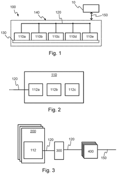
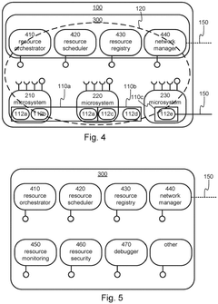
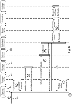
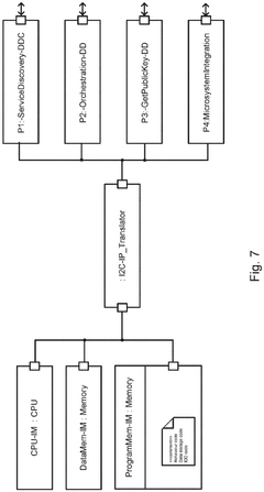
- A chiplet arrangement with a control plane that orchestrates microsystems and microservices, allowing for dynamic instantiation based on hardware resource availability and utilization, featuring a resource orchestrator, network manager, and resource scheduler to optimize resource utilization, scalability, and power management.
Supply Chain Implications of Chiplet Adoption
The adoption of chiplet technology in semiconductor manufacturing is poised to significantly impact the industry's supply chain dynamics. As chiplets allow for the disaggregation of complex system-on-chip (SoC) designs into smaller, more manageable components, the traditional monolithic approach to chip production is being challenged. This shift is expected to create new opportunities and challenges for various players in the semiconductor supply chain.
One of the primary implications of chiplet adoption is the potential for increased specialization among semiconductor manufacturers. As different chiplets can be produced using different process nodes, foundries may focus on optimizing specific manufacturing processes rather than attempting to excel across all nodes. This specialization could lead to a more diverse and resilient supply chain, with multiple suppliers capable of producing specific chiplet components.
The chiplet approach also introduces new challenges in terms of integration and packaging. As chiplets from different manufacturers need to be assembled into a single package, there is a growing demand for advanced packaging technologies and expertise. This trend is likely to boost the importance of outsourced semiconductor assembly and test (OSAT) companies in the supply chain, potentially leading to increased investment and innovation in this sector.
Furthermore, the adoption of chiplets may alter the relationship between chip designers and manufacturers. With the ability to mix and match chiplets from different sources, chip designers may have more flexibility in choosing manufacturing partners. This could potentially reduce dependency on a single manufacturer and foster greater competition in the foundry market.
The chiplet ecosystem also necessitates the development of new standards and interfaces to ensure interoperability between different chiplets. This requirement is driving collaboration across the industry, potentially leading to the formation of new alliances and partnerships. Such collaborations could reshape the competitive landscape and influence the distribution of value across the supply chain.
Lastly, the chiplet approach may impact the geographical distribution of semiconductor manufacturing. As different components can be produced in various locations and then integrated, it could potentially lead to a more globally distributed supply chain. This distribution might help mitigate some of the geopolitical risks associated with the concentration of semiconductor manufacturing in specific regions.
Chiplet Standards and Ecosystem Development
The development of chiplet standards and ecosystems is crucial for the widespread adoption and success of chiplet technology in semiconductor manufacturing. As the industry moves towards disaggregated chip designs, standardization efforts are gaining momentum to ensure interoperability and compatibility across different chiplet implementations.
Several industry consortia and organizations are actively working on establishing chiplet standards. The Universal Chiplet Interconnect Express (UCIe) consortium, formed in 2022, is leading the charge in developing open standards for die-to-die interconnects. UCIe aims to create a unified ecosystem that enables chiplets from different vendors to work seamlessly together, fostering innovation and competition in the semiconductor industry.
Another significant player in chiplet standardization is the Open Compute Project (OCP), which has been working on the Open Domain-Specific Architecture (ODSA) initiative. The ODSA focuses on creating open interfaces and protocols for chiplet-based systems, with a particular emphasis on data center applications.
The ecosystem development around chiplets involves collaboration between various stakeholders, including semiconductor manufacturers, packaging companies, and electronic design automation (EDA) tool providers. Major chip manufacturers like Intel, AMD, and TSMC are investing heavily in chiplet technology and contributing to the development of standards and ecosystem support.
EDA companies are also playing a crucial role in the chiplet ecosystem by developing tools and methodologies for chiplet-based design. These tools enable designers to effectively partition complex systems into multiple chiplets, optimize interconnects, and manage thermal and power considerations specific to chiplet architectures.
The emergence of chiplet marketplaces is another important aspect of ecosystem development. These platforms aim to facilitate the exchange of chiplet designs and intellectual property (IP) between different companies, potentially accelerating innovation and reducing development costs.
As the chiplet ecosystem matures, we can expect to see increased collaboration between foundries, packaging houses, and design houses. This collaboration will be essential for addressing challenges related to known-good-die testing, thermal management, and system-level optimization of chiplet-based designs.
The success of chiplet standards and ecosystem development will have far-reaching implications for the semiconductor industry. It has the potential to democratize chip design, enable more specialized and efficient computing solutions, and drive innovation in areas such as artificial intelligence, edge computing, and high-performance computing.
Unlock deeper insights with Patsnap Eureka Quick Research — get a full tech report to explore trends and direct your research. Try now!
Generate Your Research Report Instantly with AI Agent
Supercharge your innovation with Patsnap Eureka AI Agent Platform!