Why Engineering Drive Resistive RAM Market Changes
OCT 9, 20259 MIN READ
Generate Your Research Report Instantly with AI Agent
PatSnap Eureka helps you evaluate technical feasibility & market potential.
ReRAM Technology Evolution and Objectives
Resistive Random Access Memory (ReRAM) has emerged as a promising next-generation non-volatile memory technology over the past two decades. The evolution of ReRAM technology can be traced back to the early 2000s when researchers first observed resistive switching phenomena in various oxide materials. This discovery laid the foundation for developing memory devices that store information by changing the resistance state of a material rather than storing charge.
The technological trajectory of ReRAM has been characterized by significant advancements in material science, device architecture, and fabrication processes. Initially, simple metal-insulator-metal structures were used, but as understanding deepened, more sophisticated designs incorporating multiple layers and novel materials have been developed to enhance performance metrics such as endurance, retention, and switching speed.
Market dynamics have played a crucial role in shaping ReRAM's evolution. The increasing demand for faster, more energy-efficient memory solutions in applications ranging from Internet of Things (IoT) devices to data centers has accelerated research and development efforts. The limitations of traditional memory technologies like DRAM and NAND flash, particularly in terms of scaling and power consumption, have created a technological gap that ReRAM aims to fill.
Engineering innovations have been the primary drivers of ReRAM market changes. Breakthroughs in addressing key technical challenges such as variability, reliability, and yield have gradually improved ReRAM's commercial viability. The development of innovative selector devices to mitigate sneak path issues in crossbar arrays represents one such critical engineering advancement that has expanded ReRAM's potential application scope.
The primary objectives of current ReRAM technology development are multifaceted. First, achieving higher density through improved scaling capabilities remains a priority to compete with established memory technologies. Second, enhancing reliability and endurance to meet the stringent requirements of enterprise storage applications is crucial. Third, reducing manufacturing costs through process optimization and compatibility with standard CMOS fabrication techniques is essential for mass market adoption.
Looking forward, the convergence of ReRAM with emerging computing paradigms such as neuromorphic computing and in-memory computing represents a significant evolution path. ReRAM's inherent characteristics make it particularly suitable for these applications, potentially enabling more efficient AI systems and edge computing solutions. This alignment with future computing needs is reshaping market expectations and driving investment in specialized ReRAM variants optimized for these novel use cases.
The technology evolution trajectory suggests that ReRAM is approaching an inflection point where engineering improvements may soon translate into significant market penetration, particularly in specialized applications where its unique advantages outweigh the established incumbents.
Market Demand Analysis for ReRAM Solutions
The global market for Resistive Random Access Memory (ReRAM) solutions is experiencing significant growth driven by increasing demands across multiple sectors. Current market analysis indicates that the ReRAM market is projected to grow substantially through 2030, with particularly strong adoption in edge computing, Internet of Things (IoT) devices, and artificial intelligence applications.
The primary market demand for ReRAM stems from its unique value proposition in addressing the limitations of conventional memory technologies. Data centers and cloud computing infrastructure providers are actively seeking energy-efficient memory solutions to reduce operational costs and carbon footprint. ReRAM's low power consumption characteristics position it as an attractive alternative to traditional DRAM and flash memory in these environments.
In the consumer electronics sector, demand is being fueled by the need for faster, more energy-efficient devices with improved battery life. Smartphone manufacturers are exploring ReRAM integration to enable enhanced user experiences while maintaining competitive battery performance. The automotive industry represents another significant growth vector, with advanced driver-assistance systems (ADAS) and autonomous vehicles requiring robust, high-endurance memory solutions capable of operating reliably in extreme conditions.
Industrial IoT applications are creating substantial demand for ReRAM solutions due to their requirement for non-volatile memory with high write endurance and radiation hardness. Smart manufacturing systems, which process vast amounts of sensor data at the edge, benefit from ReRAM's ability to perform in-memory computing, reducing latency and power consumption in critical industrial processes.
The healthcare and medical device sectors are emerging as promising markets for ReRAM technology. Wearable health monitors, implantable medical devices, and point-of-care diagnostic equipment all require reliable, low-power memory solutions with long operational lifespans. ReRAM's radiation resistance also makes it particularly valuable for medical imaging equipment.
Market research indicates that enterprise customers are increasingly prioritizing sustainability in their technology procurement decisions. ReRAM's energy efficiency aligns with these environmental considerations, creating additional market pull. Furthermore, the growing trend toward edge AI and machine learning is creating demand for memory architectures that can efficiently handle neural network operations, an area where ReRAM's analog computing capabilities offer significant advantages.
Regional analysis shows particularly strong demand growth in Asia-Pacific markets, where semiconductor manufacturing is concentrated, and in North America, where early adoption of emerging technologies is common. The European market shows increasing interest driven by industrial automation applications and stringent energy efficiency regulations.
ReRAM Technical Challenges and Global Development Status
Resistive RAM (ReRAM) technology faces several significant technical challenges that have influenced its global development trajectory. The primary obstacle remains the uniformity and reliability of switching behavior across large arrays, with device-to-device and cycle-to-cycle variations presenting major hurdles for commercial deployment. These variations stem from the stochastic nature of filament formation and rupture processes, which are difficult to control precisely at nanoscale dimensions.
Material interface engineering represents another critical challenge, as the electrode-oxide interface properties substantially impact ReRAM performance characteristics. Researchers worldwide are investigating various material combinations to optimize retention, endurance, and switching speed while maintaining CMOS compatibility. The trade-off between retention time and switching speed continues to be a fundamental limitation requiring innovative solutions.
Scaling issues also persist as ReRAM cells approach sub-20nm dimensions, where quantum effects and thermal instabilities become increasingly prominent. These effects can compromise the stability of the conductive filaments that form the basis of ReRAM operation. Additionally, the sneak path current problem in crossbar architectures necessitates the integration of selector devices, adding complexity to the fabrication process.
From a global development perspective, ReRAM research exhibits distinct regional characteristics. Asian countries, particularly Japan, South Korea, and Taiwan, lead in industrial implementation with companies like Panasonic, Samsung, and TSMC making significant investments. These regions focus primarily on high-density storage applications and embedded solutions. European research institutions concentrate on fundamental material science and novel architectures, while North American efforts are directed toward neuromorphic computing applications leveraging ReRAM's analog properties.
The technology readiness level varies considerably across different applications. ReRAM for embedded non-volatile memory has reached production maturity in specific applications, while standalone storage solutions remain at the prototype stage. Neuromorphic computing applications utilizing ReRAM are still largely in the research phase, though showing promising results in academic and industrial laboratories.
Power consumption during the SET/RESET operations presents another significant challenge, particularly for mobile and IoT applications where energy efficiency is paramount. Current solutions often require relatively high programming voltages compared to conventional memory technologies, necessitating sophisticated power management schemes.
Addressing these technical challenges requires interdisciplinary collaboration spanning materials science, device physics, circuit design, and system architecture. Recent advances in atomic layer deposition techniques, interface engineering, and pulse programming strategies have shown promise in improving ReRAM performance metrics, gradually positioning this technology as a viable alternative in the emerging non-volatile memory landscape.
Current ReRAM Engineering Solutions
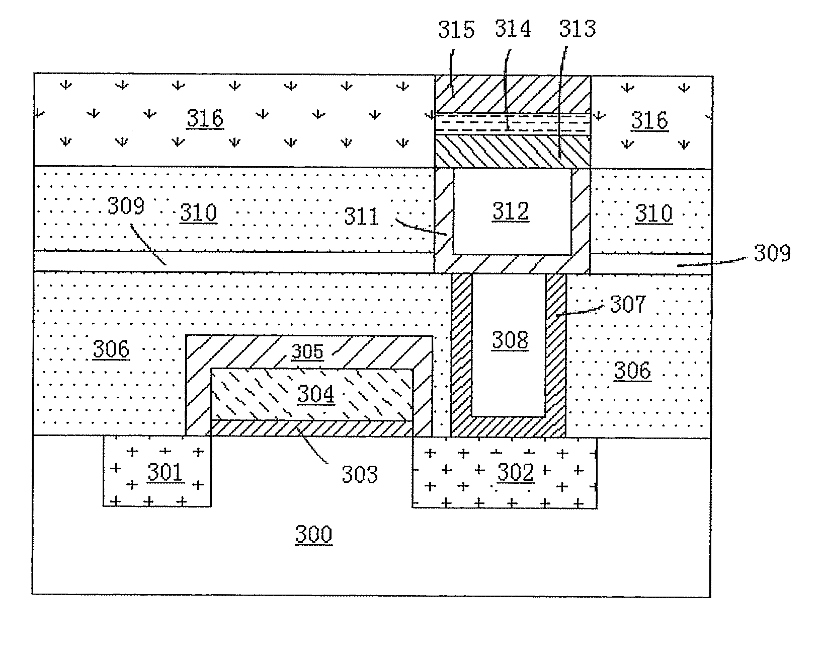
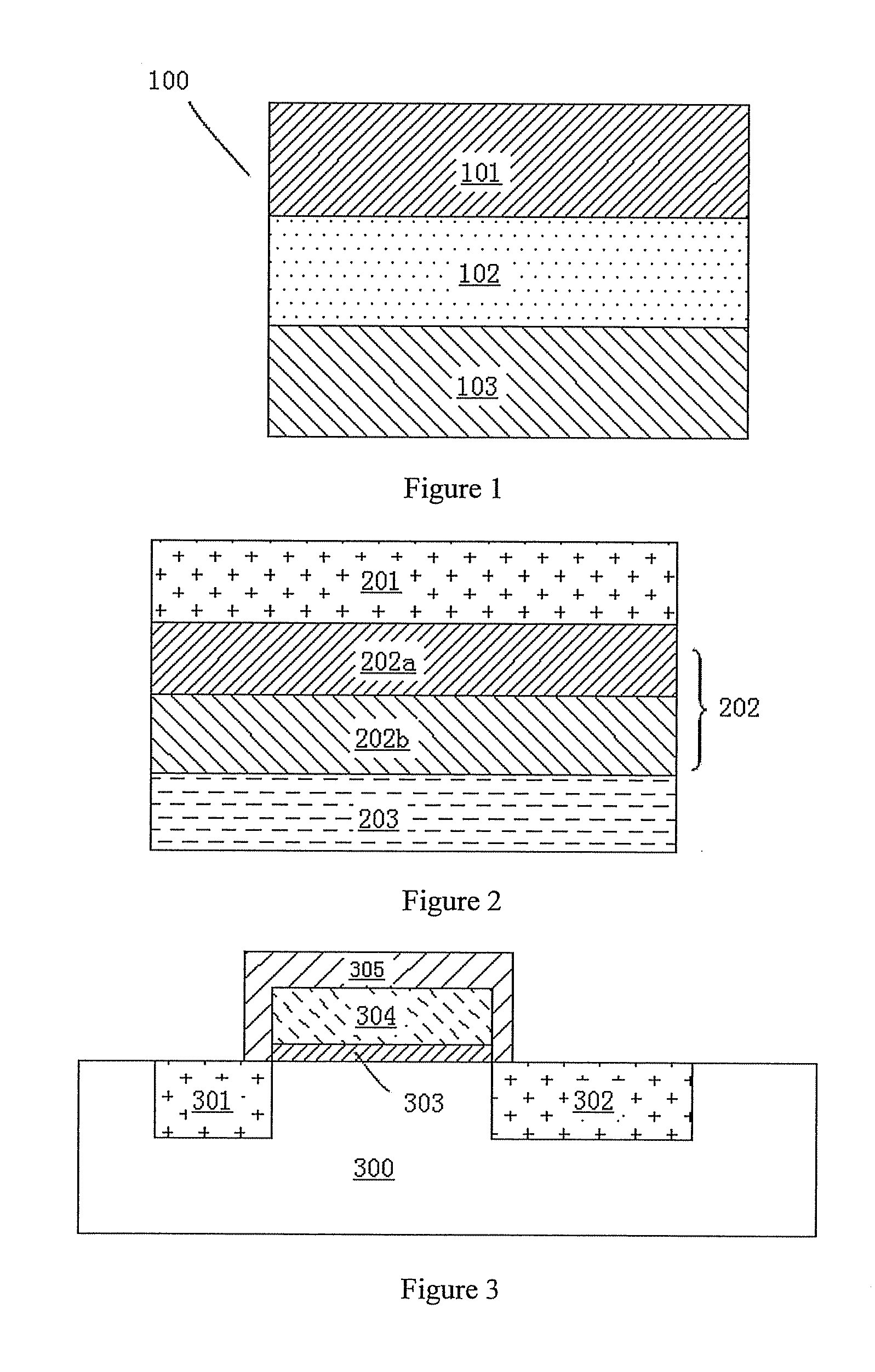
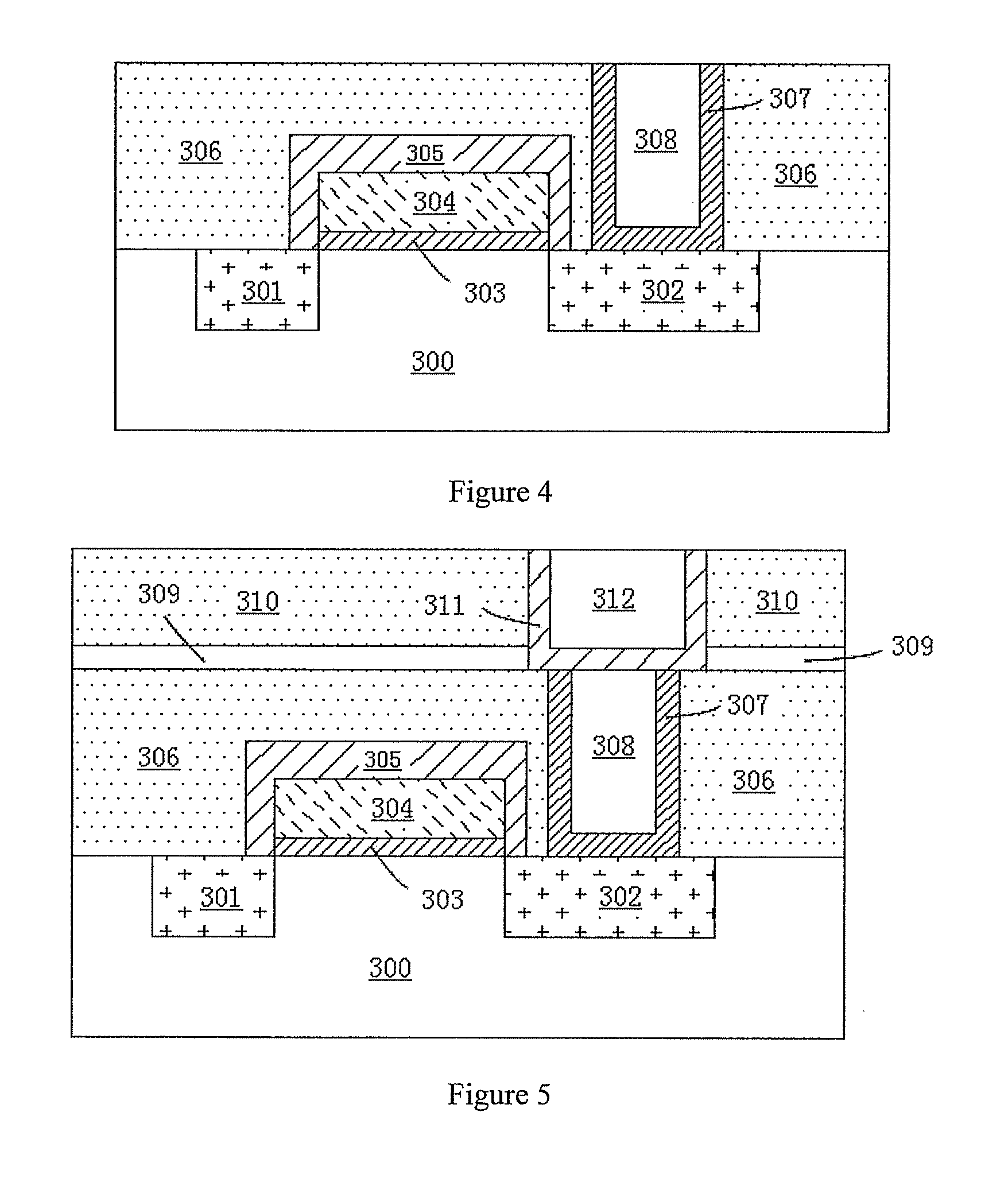
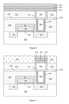
01 Resistive RAM device structures
Resistive RAM (RRAM) devices are constructed with specific structures to enable resistive switching behavior. These structures typically include a resistive switching layer sandwiched between two electrodes. The resistive switching layer can be made of various materials such as metal oxides, chalcogenides, or organic compounds. The electrode materials and their interfaces with the switching layer play crucial roles in determining the performance characteristics of the RRAM device, including switching speed, endurance, and retention time.- Materials and structures for RRAM devices: Resistive Random Access Memory (RRAM) devices utilize specific materials and structures to achieve resistive switching behavior. These typically include metal oxides like HfO2, TiO2, or Ta2O5 as the switching layer sandwiched between two electrodes. The structure may incorporate additional layers such as barrier layers or doping elements to enhance performance. The specific arrangement and composition of these materials significantly impact the device's switching characteristics, endurance, and retention properties.
- Resistive switching mechanisms: RRAM operation relies on resistive switching mechanisms where the resistance of the memory cell can be altered between high and low resistance states. This switching typically occurs through the formation and rupture of conductive filaments within the switching layer, often involving oxygen vacancies or metal ions. The switching can be categorized as unipolar or bipolar depending on the voltage polarity requirements. Understanding and controlling these mechanisms is crucial for improving device reliability and performance.
- Integration and fabrication techniques: Fabrication of RRAM devices involves various integration techniques compatible with standard semiconductor manufacturing processes. These include deposition methods such as atomic layer deposition (ALD), physical vapor deposition (PVD), or chemical vapor deposition (CVD) for the switching layer and electrodes. Advanced patterning techniques and 3D integration approaches are employed to achieve high-density memory arrays. Post-deposition treatments like annealing may be used to optimize the switching layer properties and device performance.
- Circuit design and operation methods: RRAM devices require specific circuit designs and operation methods to control the programming, erasing, and reading processes. These include sense amplifiers, write drivers, and addressing circuits. Various programming schemes such as current compliance, pulse width modulation, or multi-level programming are implemented to achieve reliable switching behavior. The circuit design must address challenges like sneak path currents in crossbar arrays and provide sufficient margins between resistance states for reliable operation.
- Applications and system integration: RRAM technology finds applications in various fields beyond conventional memory storage. These include neuromorphic computing where RRAM cells can mimic synaptic behavior, in-memory computing architectures that reduce data movement, and embedded non-volatile memory for IoT devices. System-level integration considerations include interface protocols, error correction schemes, and power management techniques. The non-volatile nature, low power consumption, and potential for high density make RRAM suitable for emerging computing paradigms and storage hierarchies.
02 Fabrication methods for Resistive RAM
Various fabrication techniques are employed to manufacture resistive RAM devices with optimal performance characteristics. These methods include physical vapor deposition, chemical vapor deposition, atomic layer deposition, and solution-based processes. The fabrication process often involves precise control of layer thicknesses, interface engineering, and post-deposition treatments such as annealing to optimize the resistive switching behavior. Advanced lithography techniques may be used to create high-density RRAM arrays for memory applications.Expand Specific Solutions03 Resistive switching mechanisms
The operation of resistive RAM relies on various switching mechanisms that cause reversible changes in resistance states. These mechanisms include filamentary conduction, where conductive filaments form and rupture within the switching layer; interface-type switching, where the resistance change occurs at the electrode-oxide interface; and phase change, where the material undergoes structural transformation between amorphous and crystalline states. Understanding these mechanisms is crucial for designing RRAM devices with improved performance, reliability, and scalability.Expand Specific Solutions04 Integration of Resistive RAM in memory architectures
Resistive RAM can be integrated into various memory architectures to leverage its advantages such as non-volatility, high density, and low power consumption. These architectures include crossbar arrays, 3D stacking, and hybrid systems that combine RRAM with conventional memory technologies. Integration challenges include addressing schemes, sneak path issues, and peripheral circuitry design. Advanced memory architectures using RRAM aim to overcome the limitations of conventional memory technologies while providing improved performance for specific applications.Expand Specific Solutions05 Applications and performance optimization of Resistive RAM
Resistive RAM finds applications in various fields including non-volatile memory, neuromorphic computing, and in-memory computing. Performance optimization techniques focus on improving key parameters such as endurance, retention time, switching speed, and power consumption. These techniques include doping of the switching layer, interface engineering, pulse shape optimization for programming and reading operations, and error correction schemes. The versatility of RRAM makes it suitable for both conventional memory applications and emerging computing paradigms.Expand Specific Solutions
Key Industry Players and Competitive Landscape
The Resistive RAM (ReRAM) market is evolving rapidly, currently transitioning from early development to commercialization phase. Major semiconductor players including Samsung, Micron, Intel, and TSMC are investing heavily in this emerging non-volatile memory technology. The market is projected to grow significantly as ReRAM offers advantages in power consumption, scalability, and endurance over traditional memory technologies. Asian manufacturers like Winbond, KIOXIA, and SMIC are particularly active, while research institutions such as IMEC and universities collaborate with industry to overcome technical challenges. The technology maturity varies across companies, with some (Intel, Micron) focusing on production-ready solutions while others (Adesto, Sharp) target specialized applications. The competitive landscape is characterized by strategic partnerships and intellectual property development as companies position themselves in this transformative memory technology market.
KIOXIA Corp.
Technical Solution: KIOXIA (formerly Toshiba Memory) has developed advanced resistive RAM technology based on their proprietary metal-oxide material system. Their ReRAM architecture employs a filamentary switching mechanism where conductive pathways form and dissolve within an insulating layer under applied voltage. KIOXIA's engineering approach focuses on reliability enhancement through specialized electrode materials and interface engineering that minimize variability between switching cycles. They have pioneered a multi-level cell (MLC) ReRAM design that stores multiple bits per cell, significantly increasing storage density while maintaining acceptable performance characteristics. Their technology demonstrates impressive specifications including sub-microsecond switching speeds, endurance ratings of 10⁵-10⁶ cycles, and retention times exceeding 10 years at operating temperatures. KIOXIA has successfully integrated their ReRAM technology with their existing flash memory manufacturing infrastructure, enabling cost-effective production. Their engineering innovations include specialized forming techniques that reduce initial power requirements and enhance device uniformity across large arrays.
Strengths: KIOXIA's extensive experience in memory manufacturing provides significant advantages in scaling ReRAM technology to commercial volumes. Their MLC approach offers compelling density improvements that address market demands for higher capacity storage. Weaknesses: Their ReRAM technology still faces challenges with cell-to-cell variability that can impact yield and reliability in large arrays. The MLC approach also introduces additional complexity in read/write circuits and error correction requirements.
Taiwan Semiconductor Manufacturing Co., Ltd.
Technical Solution: TSMC has developed embedded resistive RAM (eReRAM) technology specifically optimized for integration with their advanced logic processes. Their approach utilizes a hafnium oxide-based switching layer that demonstrates excellent compatibility with standard CMOS manufacturing flows. TSMC's ReRAM engineering focuses on ultra-low power operation, achieving write energies below 0.1pJ per bit, making it ideal for energy-constrained IoT and edge computing applications. Their technology features a 1T1R (one transistor, one resistor) cell structure that ensures reliable cell selection and minimizes disturbance issues in high-density arrays. TSMC has demonstrated successful integration of their ReRAM technology with their 22nm, 16nm, and 12nm process nodes, enabling system-on-chip designs that combine logic and non-volatile memory on the same die. Their engineering innovations include specialized forming-free designs that eliminate the need for high-voltage initialization, simplifying peripheral circuitry requirements. TSMC's ReRAM technology achieves read/write speeds of approximately 50ns/100ns respectively, with endurance ratings exceeding 10⁶ cycles and retention characteristics suitable for industrial and automotive applications.
Strengths: TSMC's position as the world's leading semiconductor foundry provides unparalleled manufacturing capabilities and process integration expertise for ReRAM technology. Their embedded approach offers significant advantages for system-level power and performance optimization. Weaknesses: As a foundry, TSMC depends on their customers to develop end products utilizing their ReRAM technology, potentially limiting their direct influence on market adoption. Their technology also faces competition from other embedded non-volatile memory options such as MRAM and eFLASH.
Critical Patents and Technical Innovations in ReRAM
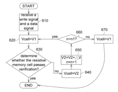
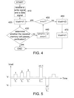
Resistive Random Access Memory and Verifying Method Thereof
PatentActiveUS20120075908A1
Innovation
- The implementation of a resistive random access memory (RRAM) system that includes a resistive memory cell, a digital-to-analog converter, a decision logic, and a selection circuit, which applies a reverse voltage to the resistive memory cell during verification failures, utilizing a reference voltage and voltage pulses to enhance the verification process.
Resistive random access memory with electric-field strengthened layer and manufacturing method thereof
PatentInactiveUS20120305880A1
Innovation
- A laminated layer structure is introduced, comprising a first resistive switching layer with a high dielectric constant and a second resistive switching and electric-field strengthened layer with a lower dielectric constant, which adjusts the electric field distribution by using materials like HfO2 and SiO2, respectively, to enhance the stability and control of conductive channels during switching.
Manufacturing Process Optimization for ReRAM
Manufacturing process optimization represents a critical frontier in advancing Resistive Random Access Memory (ReRAM) technology toward widespread commercial adoption. Current ReRAM fabrication faces significant challenges in yield rates, with typical production lines achieving only 60-75% yield compared to the 85-95% standard in mature memory technologies. This yield gap directly impacts cost structures and market competitiveness.
The integration of ReRAM cells with conventional CMOS processes requires precise control of material deposition techniques. Atomic Layer Deposition (ALD) has emerged as a preferred method for creating the critical metal oxide switching layers, offering superior uniformity and thickness control compared to traditional Physical Vapor Deposition (PVD) methods. Recent innovations in ALD chemistry have reduced deposition temperatures from 300°C to below 200°C, enabling better compatibility with back-end-of-line processing.
Electrode material selection and deposition represent another optimization frontier. The interface between electrodes and the switching layer significantly influences ReRAM performance characteristics including endurance, retention, and switching speed. Advanced manufacturing facilities have begun implementing noble metal electrodes with specialized barrier layers to prevent undesired diffusion while maintaining electrical properties.
Etching processes for ReRAM cell formation have evolved from conventional reactive ion etching to more sophisticated approaches including neutral beam etching and atomic layer etching. These techniques minimize damage to the sensitive switching materials while achieving the necessary dimensional control for high-density memory arrays. The reduction in process-induced defects has extended cell endurance from 10^6 to over 10^9 cycles in optimized production lines.
Post-fabrication treatments, including thermal annealing and electrical forming processes, have been standardized to reduce device-to-device variability. Statistical process control methodologies adapted specifically for ReRAM manufacturing have reduced switching voltage variation from ±30% to below ±10% in leading fabrication facilities. This improvement directly translates to more reliable memory operation and simplified peripheral circuitry requirements.
Equipment manufacturers have responded by developing specialized tools for ReRAM production, including multi-chamber deposition systems that allow in-situ formation of the entire memory stack without breaking vacuum. This approach minimizes contamination issues that previously plagued interface quality. Additionally, advanced metrology techniques including in-line resistivity mapping and atomic force microscopy have been integrated into production flows, enabling real-time process adjustments that maintain tight specification control.
Energy Efficiency and Sustainability Considerations
The energy consumption profile of Resistive RAM (ReRAM) represents a significant driver for market adoption in an increasingly power-conscious computing landscape. ReRAM devices demonstrate substantially lower operational power requirements compared to conventional memory technologies, with typical write operations consuming 10-100 times less energy than flash memory. This energy efficiency stems from ReRAM's fundamental switching mechanism, which requires minimal current to alter resistance states, unlike the high-voltage electron injection processes in flash memory.
In data centers, where memory systems can account for up to 40% of total power consumption, ReRAM's efficiency translates to meaningful operational cost reductions and decreased carbon footprints. The technology's non-volatile nature further enhances its sustainability profile by eliminating standby power requirements, addressing the growing concern of static power consumption in modern computing architectures.
Manufacturing considerations also favor ReRAM from a sustainability perspective. The fabrication process typically involves fewer steps and lower temperatures compared to conventional memory technologies, resulting in reduced embodied energy and carbon emissions during production. Additionally, ReRAM's material composition generally avoids rare earth elements and environmentally problematic chemicals common in other memory technologies, aligning with global initiatives to reduce electronic waste toxicity.
The extended endurance characteristics of ReRAM—with certain implementations demonstrating write cycle capabilities exceeding 10^12 operations—contribute to longer device lifespans and reduced electronic waste generation. This longevity aspect has become increasingly important as sustainability metrics gain prominence in corporate procurement decisions and regulatory frameworks.
From a system-level perspective, ReRAM's ability to enable in-memory computing architectures presents perhaps its most significant sustainability advantage. By minimizing data movement between storage and processing units, these architectures can reduce overall system energy consumption by up to 90% for certain workloads. This efficiency gain becomes particularly relevant for edge computing applications, where energy constraints often limit deployment options.
As climate change concerns intensify regulatory pressures on technology energy consumption, ReRAM's favorable energy profile positions it advantageously against competing technologies. Several major semiconductor manufacturers have already incorporated sustainability metrics into their technology roadmaps, with ReRAM frequently highlighted as a key component in meeting future energy efficiency targets.
Unlock deeper insights with PatSnap Eureka Quick Research — get a full tech report to explore trends and direct your research. Try now!
Generate Your Research Report Instantly with AI Agent
Supercharge your innovation with PatSnap Eureka AI Agent Platform!