Semiconductor chip package attached electronic device and integrated circuit module having the same

A technology of chip packaging and electronic devices, applied in the direction of electric solid devices, semiconductor devices, semiconductor/solid device components, etc., can solve the problems of inability to pattern wiring, etc., to prevent package cracks and/or welding cracks, efficient wiring, reduce The effect of small installation area

Inactive Publication Date: 2007-07-25
SAMSUNG ELECTRONICS CO LTD
View PDF1 Cites 4 Cited by
  • Summary
  • Abstract
  • Description
  • Claims
  • Application Information

AI Technical Summary

Problems solved by technology

However, in the structure of the integrated circuit module 60 shown in FIG.

Method used


Image

  • Semiconductor chip package attached electronic device and integrated circuit module having the same
  • Semiconductor chip package attached electronic device and integrated circuit module having the same
  • Semiconductor chip package attached electronic device and integrated circuit module having the same

Examples


Embodiment Construction

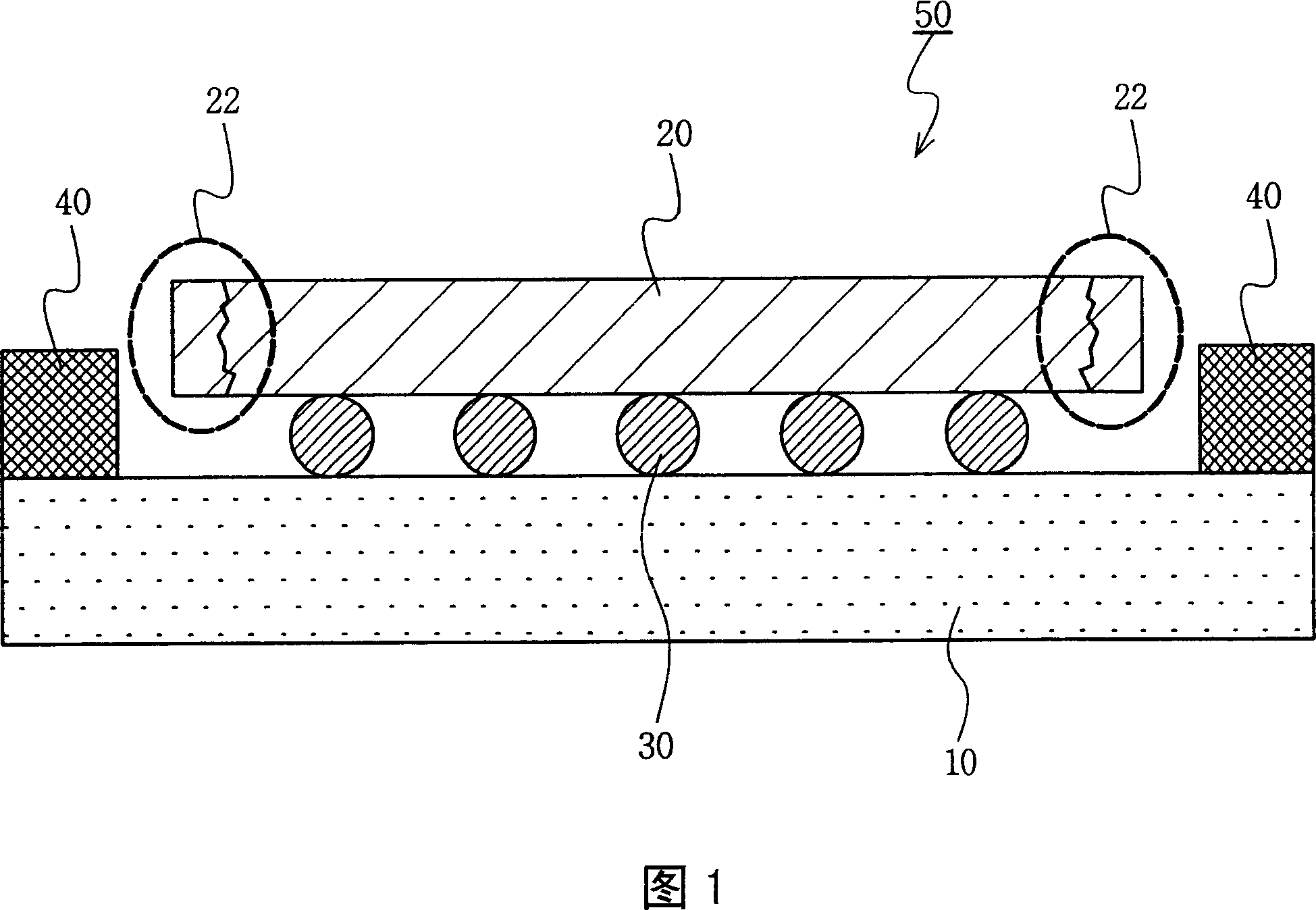
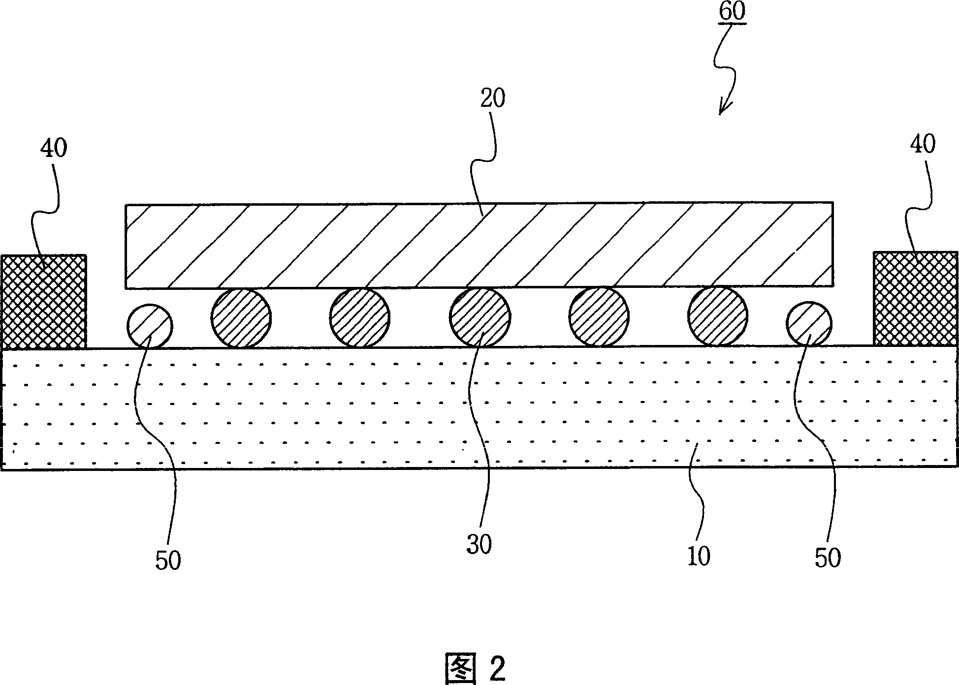
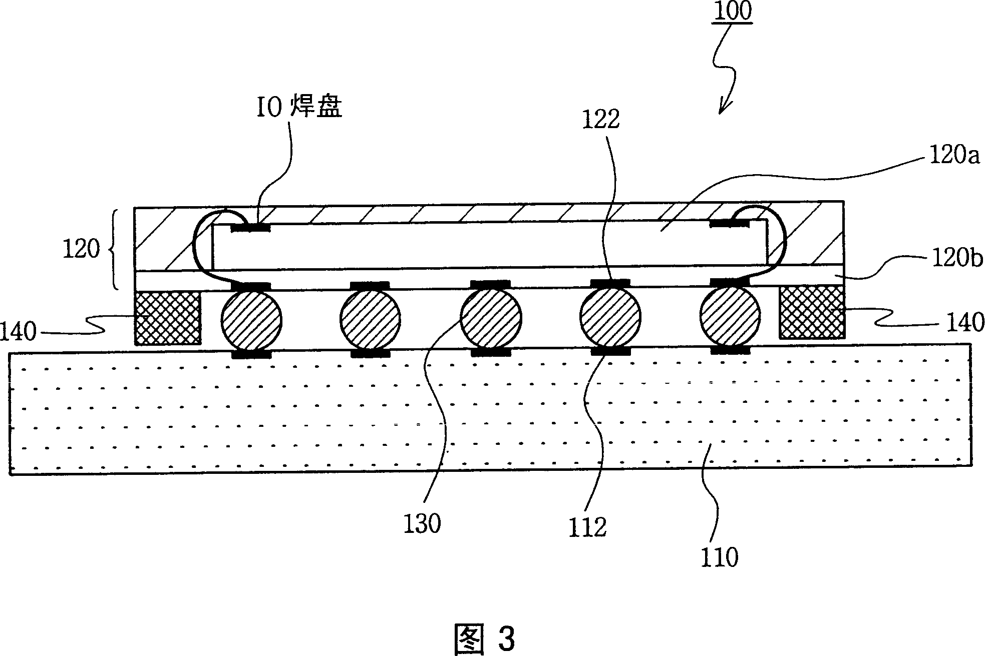
[0038] Specific descriptions of embodiments of the invention are disclosed herein. This invention may, however, be embodied in many alternative forms and should not be construed as limited to only exemplary embodiments of the invention set forth herein.

[0039] Therefore, while the exemplary embodiments of the present invention are capable of various modifications and alternative forms, the embodiments of the present invention are shown by way of example in the drawings and described in detail herein. It should be understood, however, that exemplary embodiments of the invention are not limited to the particular forms disclosed, but on the contrary, exemplary embodiments of the invention are to cover all modifications, equivalents, and alternatives falling within the scope of the invention.

[0040] Although the terms first, second, etc. are used herein to describe various elements, it will be understood that these elements should not be limited by these terms. These terms ar...


PUM


Abstract

Provided are a semiconductor chip package with attached electronic devices, and an integrated circuit module having the same. The semiconductor chip packages may include a supporting substrate, input / output bonding pads arranged on a first plane of the supporting substrate, and device bonding pads arranged on the edges of the first plane or portions of the first plane adjacent to the edges. Accordingly, the mount area of a printed circuit board may be reduced, efficient routing may be possible, and the occurrence of package cracks may be reduced and / or prevented.

Description

[0001] This application claims priority from Korean Patent Application No. 10-2006-0005275 filed on Jan. 18, 2006, the entire contents of which are hereby incorporated by reference. technical field [0002] Exemplary embodiments of the present invention relate to a semiconductor chip package with attached electronics and an integrated circuit module with the semiconductor chip package. More particularly, exemplary embodiments of the present invention relate to a semiconductor chip package with attached electronic devices and an integrated circuit module having the semiconductor chip package that reduce and / or prevent occurrence of cracks in the semiconductor chip package and reduce mounting area. Background technique [0003] Electronic products have been developed with features including small size, light weight, and high performance. Conventionally, the trend of semiconductor chip packaging for electronic products is toward providing high-performance products. Such a tren...

Claims


Application Information

Patent Timeline
Patent Type & Authority Applications(China)
IPC IPC(8): H01L25/00H01L25/16H01L23/488
CPCH05K3/303H05K2201/10378H01L2224/4824H01L23/49816H01L23/562H05K2201/1053H01L24/48H01L2224/16H05K2201/10734H05K2201/2036H01L2924/15311H05K1/0231H01L2924/19106H01L23/13H01L23/66H01L2924/19041H05K2201/10568H01L2924/181H01L2924/14H01L2924/00014Y02P70/50H01L2924/00012H01L2924/00H01L2224/45099H01L2224/45015H01L2924/207E05B1/0015A47F3/043F25D23/021F25D23/028A47B95/02F16B12/10
Inventor 金垌宣高基显吴秉夏
Owner SAMSUNG ELECTRONICS CO LTD
Why Eureka
Try Eureka