3D (3-dimensional) touch liquid crystal lens grating, display device and manufacturing methods of 3D touch liquid crystal lens grating and display device

A technology of a liquid crystal lens and a manufacturing method, applied in optics, optical elements, nonlinear optics, etc., can solve the problems of increasing production costs, large thickness of display devices, complicated processing and manufacturing of display devices, etc. The effect of simplifying the production process

Active Publication Date: 2012-10-03
BEIJING BOE OPTOELECTRONCIS TECH CO LTD
View PDF5 Cites 42 Cited by
  • Summary
  • Abstract
  • Description
  • Claims
  • Application Information

AI Technical Summary

Problems solved by technology

Compared with the traditional 3D display device, the 3D touch display device with such a structure has a larger overall thickness of the display device. Excessive box thick

Method used


Image

  • 3D (3-dimensional) touch liquid crystal lens grating, display device and manufacturing methods of 3D touch liquid crystal lens grating and display device
  • 3D (3-dimensional) touch liquid crystal lens grating, display device and manufacturing methods of 3D touch liquid crystal lens grating and display device
  • 3D (3-dimensional) touch liquid crystal lens grating, display device and manufacturing methods of 3D touch liquid crystal lens grating and display device

Examples


Example Embodiment

[0026] The following will clearly and completely describe the technical solutions in the embodiments of the present invention with reference to the accompanying drawings in the embodiments of the present invention. Obviously, the described embodiments are only some, not all, embodiments of the present invention. Based on the embodiments of the present invention, all other embodiments obtained by persons of ordinary skill in the art without making creative efforts belong to the protection scope of the present invention.

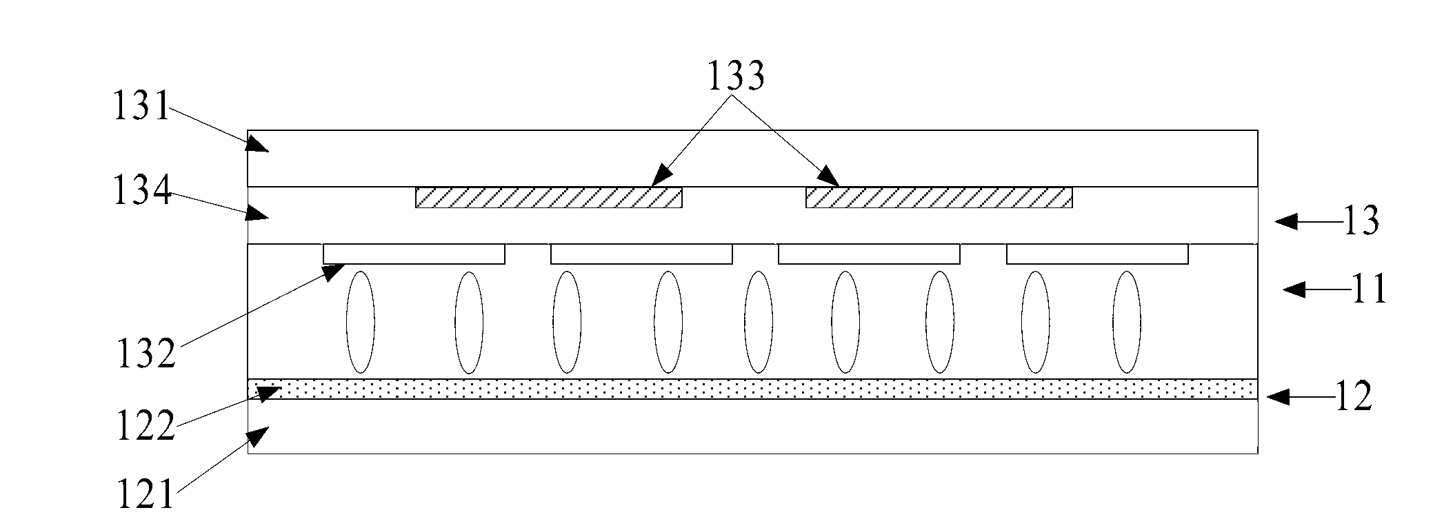
[0027] The 3D touch liquid crystal lens grating provided by the embodiment of the present invention, such as figure 1 As shown, the 3D touch liquid crystal lens grating 11 includes:

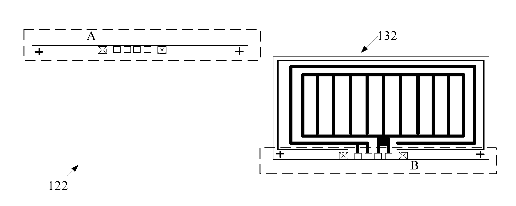
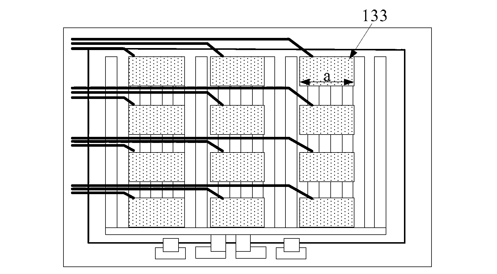
[0028] The lower substrate 12 and upper substrate 13 molded to the box, the lower substrate 12 includes a lower transparent substrate 121 and a surface electrode 122, the upper substrate 13 includes an upper transparent substrate 131 and a strip electrode 132, and the space betwe...


PUM


Abstract

The embodiment of the invention provides a 3D (3-dimensional) touch liquid crystal lens grating, display device and manufacturing methods of the 3D touch liquid crystal lens grating and the display device and relates to the technical field of display, and the thickness of the 3D touch display device can be reduced. The 3D touch liquid crystal lens grating comprises a lower substrate and an upper substrate, wherein the lower substrate and the upper substrate are formed by box-box molding; the lower substrate comprises a lower transparent substrate and a surface electrode; the upper substrate comprises an upper transparent substrate a strip-shaped electrode; liquid crystal is filled between the surface electrode and the strip-shaped electrode; at least one touch electrode arranged in an adjacent mode is arranged between the upper transparent substrate and the strip-shaped electrode; and a transparent isolated cushion layer is arranged between the touch electrode and the strip-shaped electrode. A double-layer electrode used for touch in the prior art can be reduced to a single-layer electrode by the embodiment of the invention, thus the thickness of the 3D touch display device is reduced, the manufacturing process is simplified, and the production cost of a product is reduced.

Description

technical field [0001] The invention relates to the field of display technology, in particular to a 3D touch liquid crystal lens grating, a display device and a manufacturing method thereof. Background technique [0002] With the development of display technology, 3D (Three Dimensions, three-dimensional graphics) display devices with stereoscopic display effects and touch screens supporting touch control are increasingly sought after by consumers. Integrated products with both 3D display and touch screen touch functions are attracting more and more people's attention. [0003] At present, display devices with both 3D display and touch screen support functions are usually obtained by superposition, that is, the double-layer electrodes for touch control are additionally processed on the 3D display device that has been formed into a box. Compared with the traditional 3D display device, the 3D touch display device with such a structure has a larger overall thickness of the disp...

Claims


Application Information

Patent Timeline
IPC IPC(8): G02F1/1343G02F1/133G02F1/1335G02F1/29G02B27/22G06F3/041G02B30/28
CPCH04N13/04G02F1/1333G02F1/13338G06F2203/04103G02F1/1341H04N13/0404G02B27/2214G06F3/0412G02F2201/44H04N13/305Y10T29/4913G06F3/0445G02B30/28H04N13/30G02F1/13G09G3/34G02B30/00G02B30/27
Inventor 杨盛际吴俊伟王海生刘英明
Owner BEIJING BOE OPTOELECTRONCIS TECH CO LTD
Why Eureka
Try Eureka