Touch display screen and touch display device

A touch display and shielding layer technology, applied in optics, instruments, electrical and digital data processing, etc., can solve the problem of difficult to achieve touch effects, achieve both anti-static properties and touchability, and ensure achievability. , improve the display effect

Inactive Publication Date: 2013-03-06
BEIJING BOE OPTOELECTRONCIS TECH CO LTD
View PDF3 Cites 25 Cited by
  • Summary
  • Abstract
  • Description
  • Claims
  • Application Information

AI Technical Summary

Problems solved by technology

[0006] The invention provides a touch display screen and a touch display device, which are used to solve the problem that the projected electric field signal between the drive electrode line and the detection electrode line of the existing touch display screen is blocked by a planar shielding layer, and the touch effect is difficult to achieve technical issues

Method used


Image

  • Touch display screen and touch display device

Examples


Embodiment Construction

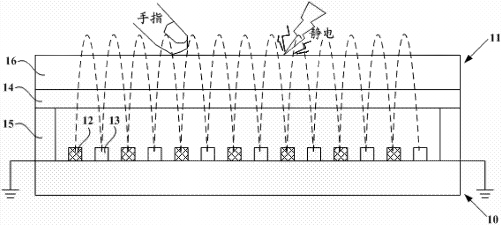
[0025] In order to solve the technical problem that the projected electric field signal between the drive electrode line and the detection electrode line of the existing touch screen is blocked by the planar shielding layer, and the touch effect is difficult to achieve, the embodiment of the present invention provides a touch screen and touch display device. In the technical solution of the present invention, a high-resistance transparent conductive shielding layer is provided on the color filter substrate. The shielding layer is located on a set of first electrode lines and a set of second electrode lines. Due to its high resistance characteristics, the first The projected electric field signal between the electrode line and the second electrode line passes through it, which ensures the achievability of touch operation. At the same time, due to the conductive characteristics of the shielding layer, it can avoid electrostatic damage to the display screen caused by electrostatic...


PUM


Abstract

The invention discloses a touch display screen and a touch display device. The touch display screen comprises an array substrate, a color film substrate, a group of first electrode lines, a group of second electrode lines and high-resistance transparent conductive shielding layers, wherein the array substrate and the color film substrate are symmetrically arranged; the group of first electrode lines is arranged on the array substrate or the color film substrate; the group of second electrode lines is arranged on the array substrate or the color film substrate and is in intersection arrangement with the group of first electrode lines; and the high-resistance transparent conductive shielding layers are arranged on the color film substrate and are positioned on the group of first electrode lines and the group of second electrode lines. The resistance value of the high-resistance transparent conductive shielding layers is higher, thus projection electric field signals between the first electrode lines and the second electrode lines can pass through the high-resistance transparent conductive shielding layers, and the implementability of touch operation is ensured; and in addition, the transparent conductive shielding layers per se have conductivity, when a display screen is touched by external static electricity, electrostatic charges can be quickly led out and connected with the ground by the transparent conductive shielding layers, the electrostatic damage to the display screen due to the electrostatic charges can be prevented, and the display effect is further increased.

Description

technical field [0001] The present invention relates to the technical field of touch display, in particular to a touch display screen and a touch display device. Background technique [0002] At present, most mutual capacitive touch screens are plug-in, that is, the touch screen and the display screen are manufactured separately and then bonded together. This technology has the disadvantages of high production cost, low light transmittance, and thick module. With the development of science and technology, embedded touch screen technology has gradually become a new favorite of research and development, which means that the driving electrode lines and detection electrode lines used to realize the touch function are arranged on the substrate of the display screen. Compared with the external touch display device, the touch display device adopting the embedded touch screen technology has the advantages of thinner thickness, wider viewing angle, higher performance and lower cost....

Claims


Application Information

Patent Timeline
Patent Type & Authority Applications(China)
IPC IPC(8): G06F3/041G02F1/1333
CPCG06F3/044G06F3/041G06F2203/04112G06F3/0412G02F1/13338G02F1/134363G06F3/0443G06F2203/04103G06F2203/04107
Inventor 丁小梁董学王海生刘英明杨盛际任涛赵卫杰刘红娟
Owner BEIJING BOE OPTOELECTRONCIS TECH CO LTD
Why Eureka
Try Eureka