Semiconductor radiation detector using it, and nuclear medicine diagnosis apparatus

A technology for radiation detectors and semiconductors, applied in semiconductor devices, instruments for radiological diagnosis, measuring devices, etc., can solve problems such as shortened capture length, easy to become defects, and inability to measure gamma-ray energy spectrum

Inactive Publication Date: 2013-12-04
HITACHI LTD
View PDF3 Cites 7 Cited by
  • Summary
  • Abstract
  • Description
  • Claims
  • Application Information

AI Technical Summary

Problems solved by technology

Therefore, when a lead atom enters as an impurity, it replaces a part of the thallium atoms to easily form a substitution type solid solution, and, relative to the thallium atom, it is easy to become a valence, and the lead atom is easy to become a valence, so the part replaced by the lead atom is easy to form a crystal. become a defect
In order to make the thallium bromide crystal work as a semiconductor radiation detector and obtain high energy resolution, it is necessary to collect most of the charge carriers generated by the passage of the incident radiation, but in the crystal formed by the substitution of lead atoms In the defect, the charge carrier is trapped and the trapping length becomes short, and it can be considered that the γ-ray energy spectrum of 122keV and 662keV cannot be measured

Method used


Image

  • Semiconductor radiation detector using it, and nuclear medicine diagnosis apparatus
  • Semiconductor radiation detector using it, and nuclear medicine diagnosis apparatus
  • Semiconductor radiation detector using it, and nuclear medicine diagnosis apparatus

Examples


Embodiment Construction

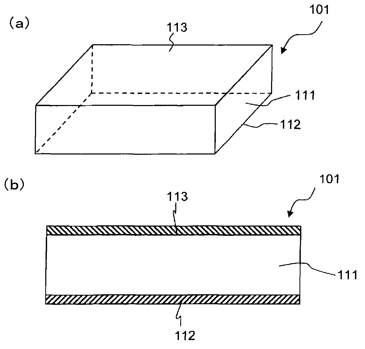
[0030] Below, use Figure 1 to Figure 8 The structure and operation of a semiconductor radiation detector according to an embodiment of the present invention and a nuclear medicine diagnostic apparatus using the same will be described.

[0031] First, use figure 1 The structure of the semiconductor radiation detector of this embodiment will be described.

[0032] figure 1 It is a configuration diagram of a semiconductor radiation detector according to an embodiment of the present invention. figure 1 (a) is a stereogram, figure 1 (b) is a sectional view.

[0033] The semiconductor radiation detector (hereinafter, simply referred to as “detector”) 101 of this embodiment includes: a semiconductor crystal 111 formed in a flat plate shape; a first electrode 112 disposed on one surface (lower surface) of the semiconductor crystal 111; And the second electrode 113 arranged on the other surface (upper surface).

[0034]The semiconductor crystal 111 forms a region where charges a...


PUM


Abstract

The present invention to provide a measurement of 122keV and 662keV Gamma-ray energy spectrum using the semiconductor radiation detector and its nuclear medicine diagnosis apparatus. A semiconductor radiation detector (101) used by the cathode (112) and the anode (113) sandwiched between the semiconductor crystal (113) is made. Semiconductor crystal (111) single crystal by thallium bromide as an impurity concentration of less than 0.1ppm of lead configuration. Due to the small concentration of a single crystal of thallium bromide, lead atoms, it is possible to lead atoms thallium atoms replaced with the density of defects in the crystal is small, the charge carriers can be extended to capture length, therefore, as the radiation detector, can be measured with high energy resolution and Gamma-ray energy spectrum of 662keV and 122keV.

Description

technical field [0001] The present invention relates to a semiconductor radiation detector and a nuclear medicine diagnostic device using the same. Background technique [0002] In recent years, nuclear medicine diagnostic devices using radiation detectors that measure rays such as gamma rays have been widely used. Typical nuclear medicine diagnostic devices include a gamma radiation chamber, a single photon emission tomography (SPECT (Single Photon Emission Computed Tomography) imaging device), a positron emission tomography (PET (Positron Emission Tomography) imaging device), and the like. In addition, in dosimeters for countermeasures against radioactive bombs and the like using radiation detectors, the demand for radiation detectors for homeland security is increasing. [0003] In the past, although these radiation detectors combined scintillators and photomultiplier tubes, in recent years, technologies using semiconductor radiation detectors composed of semiconductor c...

Claims


Application Information

Patent Timeline
Patent Type & Authority Applications(China)
IPC IPC(8): G01T1/36A61B6/03
CPCA61B6/4233H01L27/14676C30B29/12C30B11/00G01T1/24A61B6/037G01T1/249G01T1/161H01L31/032H01L31/036H01L31/0224H01L31/0264H01L31/08H01L31/085H01L31/18H01L27/14H01L27/142H01L31/115H01L31/0328C01G15/00G01T1/2928G01T1/241G01N2033/0095G01N23/22
Inventor 小南信也翁久实小桥启司
Owner HITACHI LTD
Why Eureka
Try Eureka