Image sensor packaging and manufacturing method

A technology of image sensor and manufacturing method, which is applied in the direction of electric solid-state devices, semiconductor devices, radiation control devices, etc., can solve the problems that cannot meet the miniaturization of mobile equipment, achieve the effect of reducing board erection space and enhancing competitiveness

Active Publication Date: 2014-12-24
SAMSUNG ELECTRO MECHANICS CO LTD
View PDF5 Cites 2 Cited by
  • Summary
  • Abstract
  • Description
  • Claims
  • Application Information

AI Technical Summary

Problems solved by technology

[0012] Therefore, the object of the present invention is to solve the problem that the prior art including Patent Document 1 cannot satisfy the structural miniaturization required in mobile devices.

Method used


Image

  • Image sensor packaging and manufacturing method
  • Image sensor packaging and manufacturing method
  • Image sensor packaging and manufacturing method

Examples


Embodiment Construction

[0050] According to the following specific content and embodiments associated with the accompanying drawings, the characteristics and specific technical features of the present invention will become more clear. It should be noted that, in this specification, when assigning reference numerals to constituent elements in each drawing, they are limited to the same constituent elements, and even if they are shown in different drawings, they are assigned the same reference numerals as much as possible. In addition, terms such as "first", "second", "one side", and "the other side" are used to distinguish one constituent element from other constituent elements, and the constituent elements are not limited by the terms. In describing the present invention, detailed descriptions of related well-known technologies that would unnecessarily obscure the gist of the present invention will be omitted.

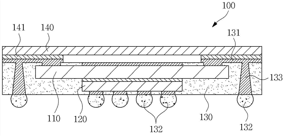
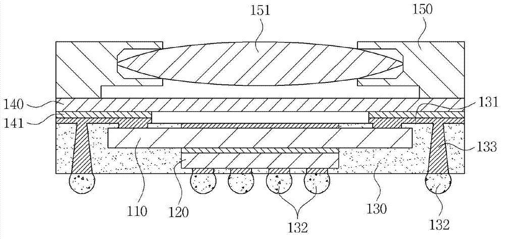
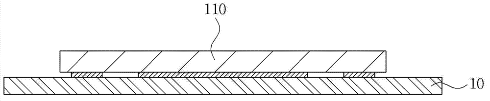
[0051] The image sensor package (Image Sensor Package) of the embodiment of the present in...


PUM


Abstract

The invention relates to image sensor packaging and a manufacturing method. An image senor and a device are formed by lamination structures. Then packaging is carried out by utilization of thermosetting resins through molding. The area of the device can be increased easily. In addition, a substrate used in precious image senor packaging manufacturing process can be removed easily and therefore the miniaturization requirement in a mobile device can be met.

Description

technical field [0001] The present invention relates to image sensor packages and methods of manufacturing the same. Background technique [0002] With regard to the packaging (packaging) of devices (Device) used in mobile (Mobile) devices such as smartphones and tablet PCs, miniaturization and high performance have been demanded. In addition, efforts are being made to add more functions in the same space or to increase battery capacity as much as possible in the remaining space by miniaturizing the package. [0003] In particular, for parts with additional functions that are not main parts, there is a stronger demand for miniaturization, which is sometimes used to judge the competitiveness of manufacturers. On the other hand, along with the miniaturization trend of such mobile devices, size reduction is also constantly required for image sensor packages. [0004] Here, as is well known, a general image sensor package is a chip-on-board package (Chip) in which an image sen...

Claims


Application Information

Patent Timeline
Patent Type & Authority Applications(China)
IPC IPC(8): H01L27/146
CPCH01L25/18H01L27/14618H01L31/02005H01L31/0203
Inventor 郑泰成
Owner SAMSUNG ELECTRO MECHANICS CO LTD
Why Eureka
Try Eureka