A pixel structure, its manufacturing method, display panel and display device

A pixel structure and display device technology, applied in semiconductor devices, electrical components, circuits, etc., can solve the problem that the pixel structure cannot be compatible with ordinary display and virtual display at the same time, and achieve good visual matching effect and strong uniformity

Active Publication Date: 2018-07-17
CHONGQING BOE OPTOELECTRONICS +1
View PDF3 Cites 0 Cited by
  • Summary
  • Abstract
  • Description
  • Claims
  • Application Information

AI Technical Summary

Problems solved by technology

[0004] In view of this, an embodiment of the present invention provides a pixel structure, its manufacturing method, a display panel and a display device to solve the problem that the existing pixel structure cannot be compatible with ordinary display and virtual display at the same time

Method used


Image

  • A pixel structure, its manufacturing method, display panel and display device
  • A pixel structure, its manufacturing method, display panel and display device
  • A pixel structure, its manufacturing method, display panel and display device

Examples


specific Embodiment approach

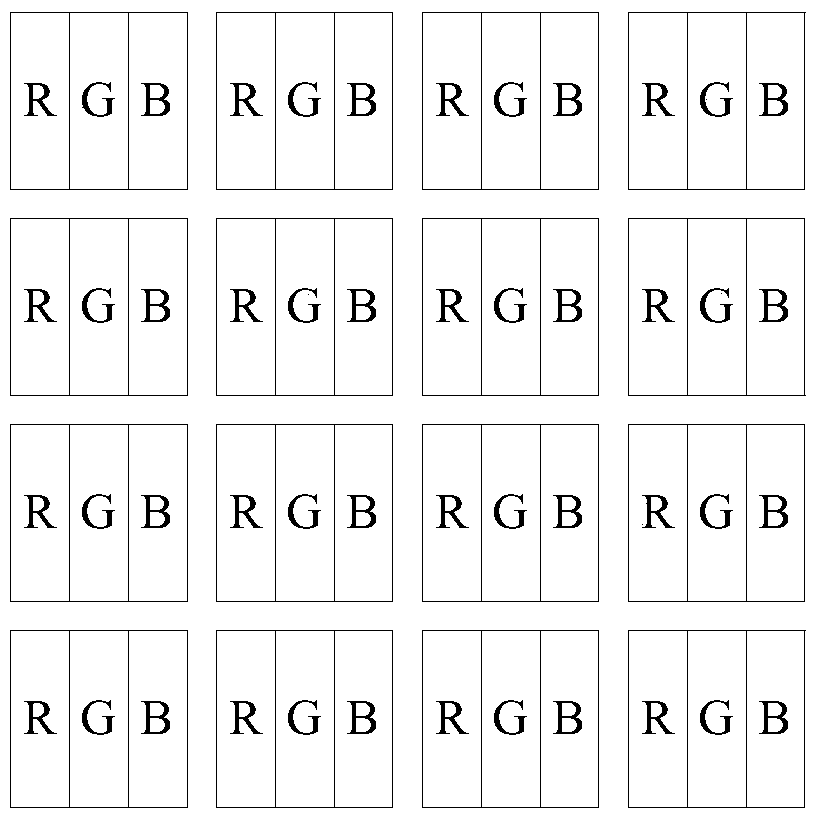
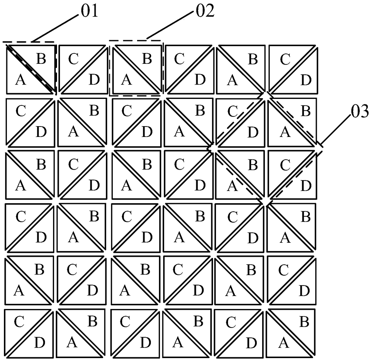
[0048] When the above-mentioned pixel structure provided by the embodiment of the present invention is arranged in a rectangular effective display area, a mask plate can be used to form color-resist patterns of sub-pixels of two colors in the pixel structure respectively. There are four sub-pixels of different colors in the pixel structure, therefore, all the color-resist patterns can be formed respectively by using two masks. Its specific implementation is as follows:

[0049] Firstly, using the first mask plate to form the color-resist pattern of the sub-pixels of the first color in the pixel structure;

[0050] Then, using the first mask rotated by 180 degrees to form the color-resist pattern of the sub-pixels of the second color in the pixel structure;

[0051] Next, using a second mask to form a color-resist pattern for the sub-pixels of the third color in the pixel structure;

[0052] Finally, the color resist pattern of the fourth color sub-pixel in the pixel structur...

Embodiment 2

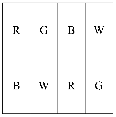
[0059] When the above-mentioned pixel structure provided by the embodiment of the present invention is set in a square effective display area, a mask plate is used to respectively form the color resistance patterns of three or four color sub-pixels in the pixel structure, wherein, a mask is used The case where the plate forms the color-resist patterns of the three-color sub-pixels in the pixel structure is the case where the color-resist patterns of the white sub-pixels do not need to be patterned. There are four sub-pixels of different colors in the pixel structure. Therefore, a mask plate is used to rotate the mask plate by 90 degrees on the basis of the previous color-resist pattern composition through the composition of each color-resist pattern. All the color resist patterns can be formed separately.

[0060] When it is necessary to make color-resisting patterns of four colors, the specific implementation method is as follows:

[0061] Firstly, using the first mask plate...


PUM


Abstract

The invention discloses a pixel structure, a manufacturing method thereof, a display panel and a display device. The pixel structure has four sub-pixels with different colors, and the shape of each sub-pixel is a right triangle. A rectangular virtual pixel; each virtual pixel is arranged in an array, and the colors of the sub-pixels contained in two adjacent virtual pixels are different; at the same time, the right angles of every four sub-pixels with different colors gather at one point to form a rhombus physical pixels, the rhombus shape of the physical pixels can also be regarded as an oblique rectangle. Since the shape of both the physical pixel and the virtual pixel in the above pixel structure is rectangular, the above pixel structure can be compatible with normal display and virtual display at the same time. Physical) pixels for low-resolution ordinary display can obtain a picture with strong uniformity and achieve a better visual matching effect.

Description

technical field [0001] The present invention relates to the field of display technology, in particular to a pixel structure, a manufacturing method thereof, a display panel and a display device. Background technique [0002] Currently, each pixel on a display panel generally consists of sub-pixels corresponding to three primary colors (red, green, and blue). When a specific color needs to be displayed, the gray value of the red (R) green (G) and blue (B) sub-pixels is adjusted to form the color. The arrangement of the sub-pixels is related to the resolution that the display panel can provide. The current common sub-pixel unit is a straight strip design, such as figure 1 shown. In order to improve the optical efficiency or display effect, a four-color display panel has been developed, that is, in addition to the three colors of RGB, it also includes white (W) pixels or yellow (Y) pixels, which are mainly based on the original pixel design. For white or yellow pixels, use ...

Claims


Application Information

Patent Timeline
Patent Type & Authority Patents(China)
IPC IPC(8): H01L27/32
CPCH10K59/122H01L27/13H10N69/00H10K59/353H10K59/351H10K71/00
Inventor 白雅杰许卓王小元金在光
Owner CHONGQING BOE OPTOELECTRONICS
Why Eureka
Try Eureka