

Reset circuit, drive method thereof, shifting register unit and grid scanning circuit
A technology of shift register and reset circuit, which is applied in the field of shift register unit, gate scan circuit, reset circuit and its drive, and can solve the problems of unable to output gate scan drive pulse normally, PU node leakage, etc.
- Summary
- Abstract
- Description
- Claims
- Application Information
AI Technical Summary
Problems solved by technology
Method used
Image

Examples
Embodiment Construction
[0031] In order to understand the above-mentioned purpose, features and advantages of the present invention more clearly, the present invention will be further described in detail below in conjunction with the accompanying drawings and specific embodiments. It should be noted that, in the case of no conflict, the embodiments of the present application and the features in the embodiments can be combined with each other.
[0032] In the following description, many specific details are set forth in order to fully understand the present invention. However, the present invention can also be implemented in other ways different from those described here. Therefore, the protection scope of the present invention is not limited by the specific details disclosed below. EXAMPLE LIMITATIONS.
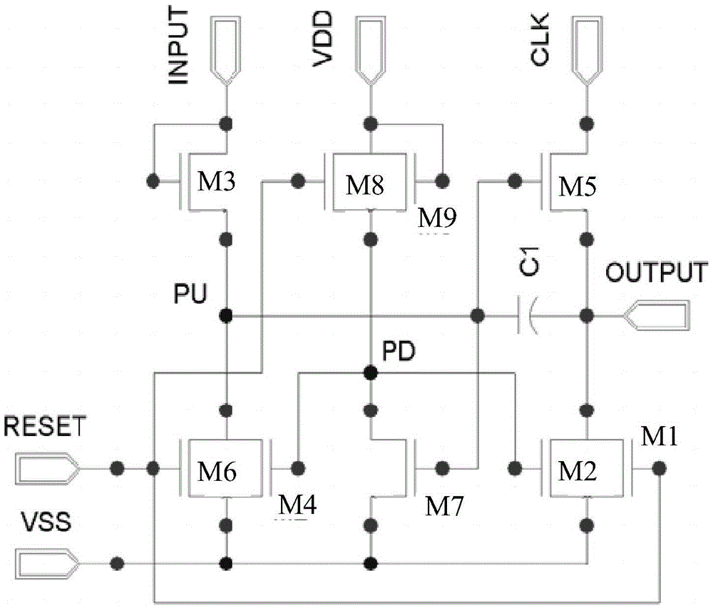
[0033] The basic structure of an existing shift register unit can refer to figure 1 , including a total of 9 N-type transistors M1-M9 and a capacitor C1, and has multiple input terminals including: ...
PUM
 Abstract
Description
Claims
Application Information