A pixel circuit, its driving method, and a display device

A technology for pixel circuits and driving modules, which is applied to circuits, electrical components, static indicators, etc., can solve problems such as unfavorable narrow frame design and occupying the area of ​​non-display areas of display devices.

Active Publication Date: 2019-05-10
BOE TECH GRP CO LTD
View PDF9 Cites 1 Cited by
  • Summary
  • Abstract
  • Description
  • Claims
  • Application Information

AI Technical Summary

Problems solved by technology

In this way, the above-mentioned camera will occupy the area of ​​the non-display area of ​​the display device, which is not conducive to the design of the narrow frame

Method used


Image

  • A pixel circuit, its driving method, and a display device
  • A pixel circuit, its driving method, and a display device
  • A pixel circuit, its driving method, and a display device

Examples


Embodiment Construction

[0030] The following will clearly and completely describe the technical solutions in the embodiments of the present invention with reference to the accompanying drawings in the embodiments of the present invention. Obviously, the described embodiments are only some, not all, embodiments of the present invention. Based on the embodiments of the present invention, all other embodiments obtained by persons of ordinary skill in the art without making creative efforts belong to the protection scope of the present invention.

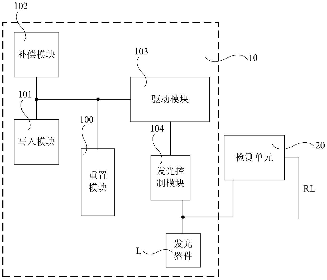
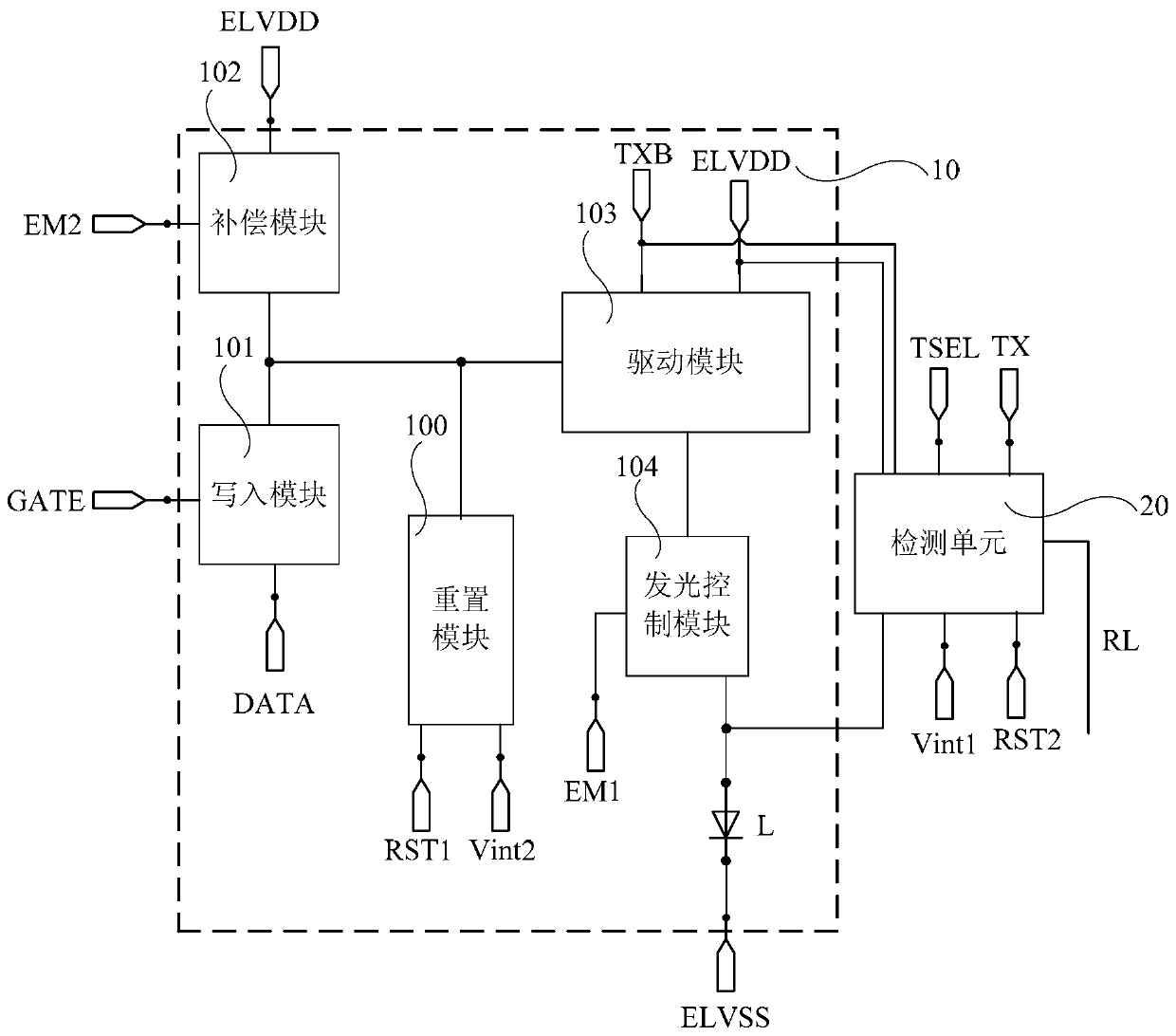
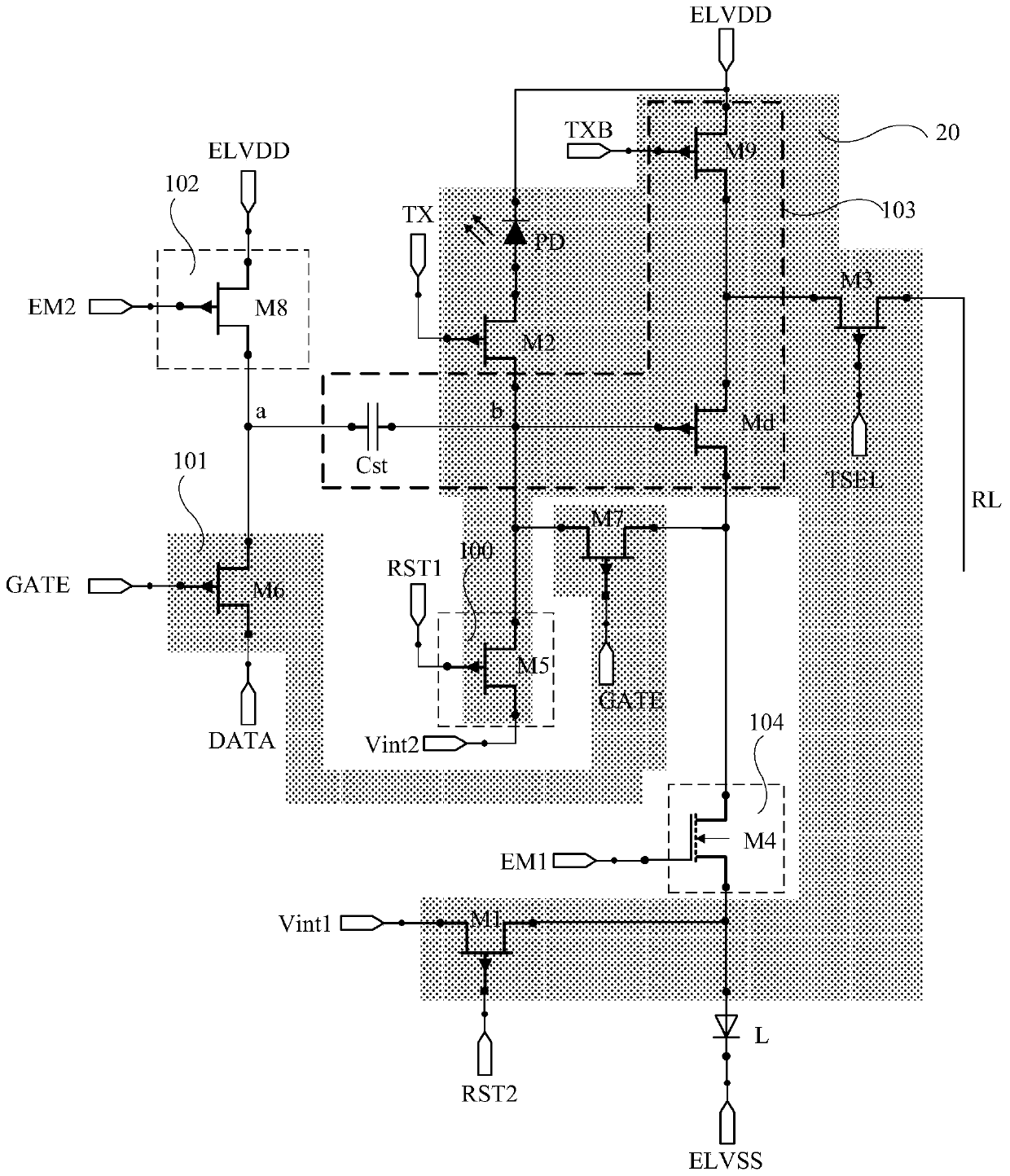
[0031] An embodiment of the present invention provides a pixel circuit, such as figure 1 As shown, a display drive unit 10 is included. The display driving unit 10 includes a reset module 100 , a writing module 101 , a compensation module 102 , a driving module 103 , a light emitting control module 104 and a light emitting device L. Wherein, the above-mentioned light emitting device L may be an LED (Light Emitting Diode, light emitting diode) or an OLED.

[...


PUM


Abstract

Embodiments of the present invention provide a pixel circuit, a driving method thereof, and a display device, which relate to the field of display technology and can prevent components with an imaging function from occupying a non-display area of ​​the display device. The pixel circuit includes a display drive unit, and the display drive unit includes a reset module, which resets the drive module; a write module, which writes data voltage into the drive module; a compensation module is connected to the threshold voltage compensation for the drive module; light emission control The module electrically connects the driving module with the light-emitting device, and provides a driving current to the light-emitting device through the driving module; the light-emitting device emits light according to the driving current. The pixel circuit also includes a detection unit, some of the transistors in the detection unit are shared with some of the transistors in the display drive unit; the detection unit collects the incident light, and outputs the collection result to the reading signal line. The above-mentioned pixel circuits are used for display and shooting.

Description

technical field [0001] The present invention relates to the field of display technology, in particular to a pixel circuit, a driving method thereof, and a display device. Background technique [0002] With the rapid progress of display technology, semiconductor element technology, which is the core of the display device, has also been greatly improved. For existing display devices, AMOLED (Active Matrix Driving Organic Light Emitting Diode, Active Matrix Driving Organic Light Emitting Diode) display devices have low manufacturing cost, high response speed, power saving, DC drive for portable devices, operating temperature Due to advantages such as large range, it is expected to become the next generation of new flat-panel displays replacing LCD (liquid crystal display, liquid crystal display). [0003] On this basis, in order to realize the camera function in the AMOLED display device, the manufacturer of the display device needs to separately purchase components with the c...

Claims


Application Information

Patent Timeline
Patent Type & Authority Patents(China)
IPC IPC(8): G09G3/3233G09G3/00
CPCG09G3/006G09G3/3233G09G2310/0262G09G2300/0861G09G2310/0251G09G2360/142G09G3/3258G09G3/3266G09G3/3275H01L27/14609H01L27/14643
Inventor 丁小梁王海生刘英明吴俊纬郑智仁王鹏鹏刘伟
Owner BOE TECH GRP CO LTD
Why Eureka
Try Eureka