Array substrate and display device

A technology for array substrates and display devices, which can be applied to instruments, optics, and electrical solid-state devices, etc., and can solve problems such as inability to perform functions, three-dimensional imaging, and gesture recognition not being applied

Active Publication Date: 2017-12-22
BOE TECH GRP CO LTD
View PDF4 Cites 12 Cited by
  • Summary
  • Abstract
  • Description
  • Claims
  • Application Information

AI Technical Summary

Problems solved by technology

But the inventor found that: at present, the functions of 3D imaging and gesture recognition have not been applied to smart display devices. For example, most touch-screen mobile phones can only receive control signals sent by users through touching the screen, but cannot Change to perform the corresponding function

Method used


Image

  • Array substrate and display device
  • Array substrate and display device
  • Array substrate and display device

Examples


Embodiment Construction

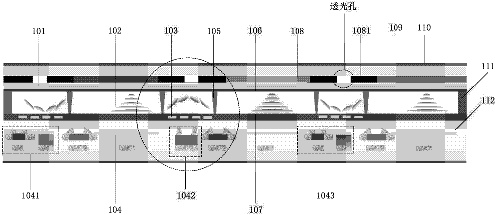
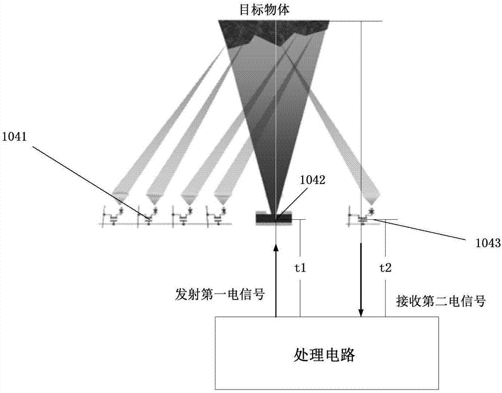
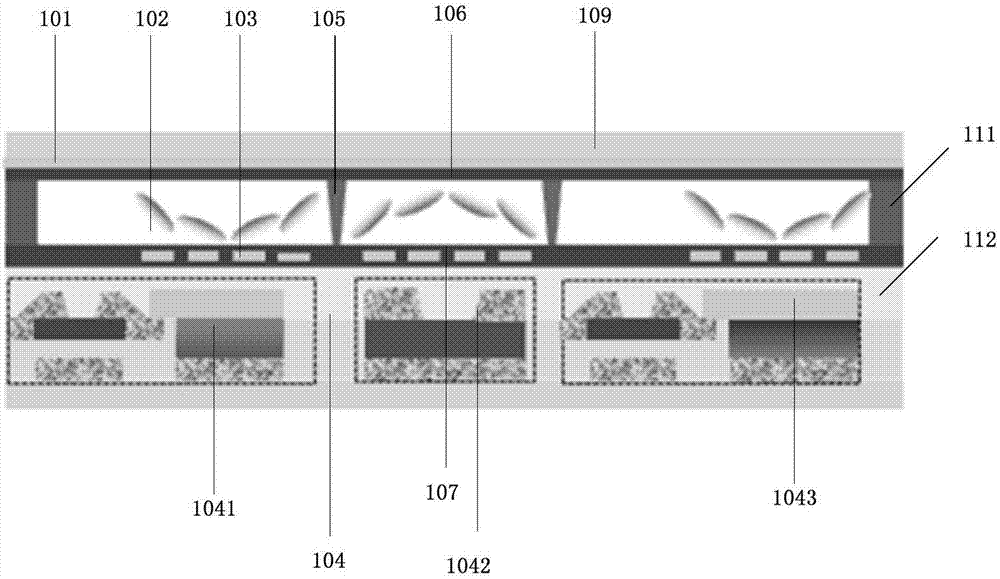
[0039] Embodiments of the present invention are described in detail below, examples of which are shown in the drawings, wherein the same or similar reference numerals designate the same or similar elements or elements having the same or similar functions throughout. The embodiments described below by referring to the figures are exemplary only for explaining the present invention and should not be construed as limiting the present invention.

[0040] Those skilled in the art will understand that unless otherwise stated, the singular forms "a", "an", "said" and "the" used herein may also include plural forms. It should be further understood that the word "comprising" used in the description of the present invention refers to the presence of said features, integers, steps, operations, elements and / or components, but does not exclude the presence or addition of one or more other features, Integers, steps, operations, elements, components, and / or groups thereof. It will be unders...


PUM


Abstract

The invention provides an array substrate and a display device. The array substrate comprises an image sensor, a light emitting diode, a photoelectric detector and a processing circuit electrically connected with the light emitting diode and the photoelectric detector. The light emitting diode is used for emitting light with a given wavelength to irradiate a target object; the image sensor is used for measuring and obtaining the light reflected by the target object and outputting two-dimensional image information; the photoelectric detector is used for receiving the light reflected by the target object and then outputting an electric signal after the light is received; the processing circuit is used for determining depth information of the target object according to the emitting moment of the light and the receiving moment of the electric signal and then determining three-dimensional image information according to the depth information and the two-dimensional image information. According to the array substrate and the display device, through arrangement of the image sensor, the light emitting diode and the photoelectric detector in each array substrate of the display device, a three-dimensional image of the target object is measured and obtained, and then the three-dimensional image is displayed.

Description

technical field [0001] The present invention relates to the display field, in particular, the present invention relates to an array substrate and a display device. Background technique [0002] With the continuous development of display technology, the functions of display devices (such as displays) are increasing. The earliest display devices only had a display function, and displayed black and white images, but the current display devices can not only display colorful images, but also become more intelligent. For example, in the current touch-screen mobile phone, the user can realize the relevant functions of the mobile phone by touching the screen, which provides convenience for the user's operation. [0003] At present, the functions of 3D imaging and gesture recognition have received extensive attention. For example, in VR (Virtual Reality, virtual reality) games, by recognizing or tracking the user's gesture changes, the user's hand is simulated into a 3D image and di...

Claims


Application Information

Patent Timeline
Patent Type & Authority Applications(China)
IPC IPC(8): G02F1/1333G02F1/1339G02F1/1337G02F1/1343G06F3/041G06F3/042
CPCG02F1/13338G02F1/1337G02F1/13394G02F1/134309G06F3/0412G06F3/0425H04N13/254H04N13/30H04N13/207G02F1/13306G02F1/13312G02F1/1339G02F1/133514G02F1/133512H01L27/14643H04N13/106H01L27/1214G02F1/1336
Inventor 秦云科董学王海生刘英明赵利军许睿郭玉珍顾品超张平贾亚楠李昌峰
Owner BOE TECH GRP CO LTD
Why Eureka
Try Eureka