A general chip test system, test method and storage medium

A chip test and chip technology, applied in the field of general chip test systems, test methods and storage media, can solve the problems of slow construction of chip test systems, inability to be generalized, and inability to share test hardware resources, so as to facilitate the rapid establishment of test systems and improve The effect of building efficiency and improving test efficiency

Active Publication Date: 2022-03-11
SHANGHAI HUALI MICROELECTRONICS CORP
View PDF17 Cites 0 Cited by
  • Summary
  • Abstract
  • Description
  • Claims
  • Application Information

AI Technical Summary

Problems solved by technology

[0011] The purpose of the present invention is to provide a general chip test system, test method and storage medium, to solve the problem of inability to share test hardware resources before and after chip tape-out, chip function evaluation, chip performance evaluation, chip Reliability evaluation and other chip test systems are slow to build and cannot be used universally

Method used


Image

  • A general chip test system, test method and storage medium
  • A general chip test system, test method and storage medium
  • A general chip test system, test method and storage medium

Examples


Embodiment Construction

[0078] In order to make the purpose, advantages and features of the present invention more clear, a general chip test system, test method and storage medium proposed by the present invention will be further described in detail below in conjunction with the accompanying drawings. Obviously, the methods described herein comprise a series of steps, and the order in which the steps are presented herein is not necessarily the only order in which the steps can be performed, and some described steps may be omitted and / or some not described herein Other steps can be added to the method. Further, the described embodiments are only some embodiments of the present invention, but not all embodiments. Based on the embodiments of the present invention, all other embodiments obtained by persons of ordinary skill in the art without making creative efforts belong to the protection scope of the present invention.

[0079]

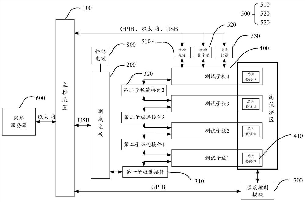
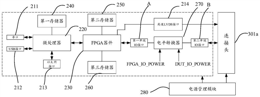
[0080] This embodiment provides a general chip test system, as attac...


PUM


Abstract

The invention provides a general chip testing system, testing method and storage medium. The chip test system includes a main control device, a test main board, N sub-board connectors, several test sub-boards and several test suites. The test main board is connected with the main control device, the test kit and the test sub-board; the test sub-board is matched with the test kit, and the test sub-board and the test main board are connected through the sub-board connector. A general-purpose chip testing system provided by the present invention can quickly and accurately verify and test the function and performance of the chip before and after design, and can meet the test tasks of function verification, performance testing, and reliability testing before chip manufacturing, and the system is The modular design has strong scalability and can realize test automation.

Description

technical field [0001] The invention relates to the technical field of chip verification testing, in particular to a general chip testing system, testing method and storage medium. Background technique [0002] As we all know, the rapid development and continuous innovation of information technology and integrated circuit technology, especially the wide application in the Internet of Things, artificial intelligence, unmanned driving, 5G and other technology industries, has brought great convenience to people's work and life and comfort. Correspondingly, people's pursuit of higher quality of work and life has also promoted the continuous development of integrated circuit technology in the direction of high precision, high speed and high reliability. [0003] The manufacturing process of integrated circuits can usually be divided into wafer manufacturing process, wafer testing, packaging and final testing. Generally, a wafer refers to a silicon wafer used to make an integrat...

Claims


Application Information

Patent Timeline
Patent Type & Authority Patents(China)
IPC IPC(8): G01R31/28
CPCG01R31/2853G01R31/2893G01R31/2855
Inventor 程景全宿晓锋郭婷武建宏
Owner SHANGHAI HUALI MICROELECTRONICS CORP
Why Eureka
Try Eureka