Wiring method and device, equipment and storage medium

A wiring method and wiring technology, applied in computer-aided design, instrumentation, electrical digital data processing, etc., can solve problems affecting wiring speed, etc.

Pending Publication Date: 2020-11-17
GUANGDONG OPPO MOBILE TELECOMM CORP LTD
View PDF0 Cites 1 Cited by
  • Summary
  • Abstract
  • Description
  • Claims
  • Application Information

AI Technical Summary

Problems solved by technology

With the shortening of the semiconductor manufacturing process, the power supply network is becoming more and more dense, and the pins of the chip unit are getting shorter and shorter. When wiring the chip unit, if the chip unit and the power supply network are distributed on different circuit layers, it may be In the case that the connection points of the pins of the chip unit are covered by the power network, the user needs to manually change the layout. Due to the large number of changes, the overall wiring speed is affected

Method used


Image

  • Wiring method and device, equipment and storage medium
  • Wiring method and device, equipment and storage medium
  • Wiring method and device, equipment and storage medium

Examples


Embodiment Construction

[0074] Before the technical solutions of the embodiments of the present invention are described in detail, the related technologies are introduced first.

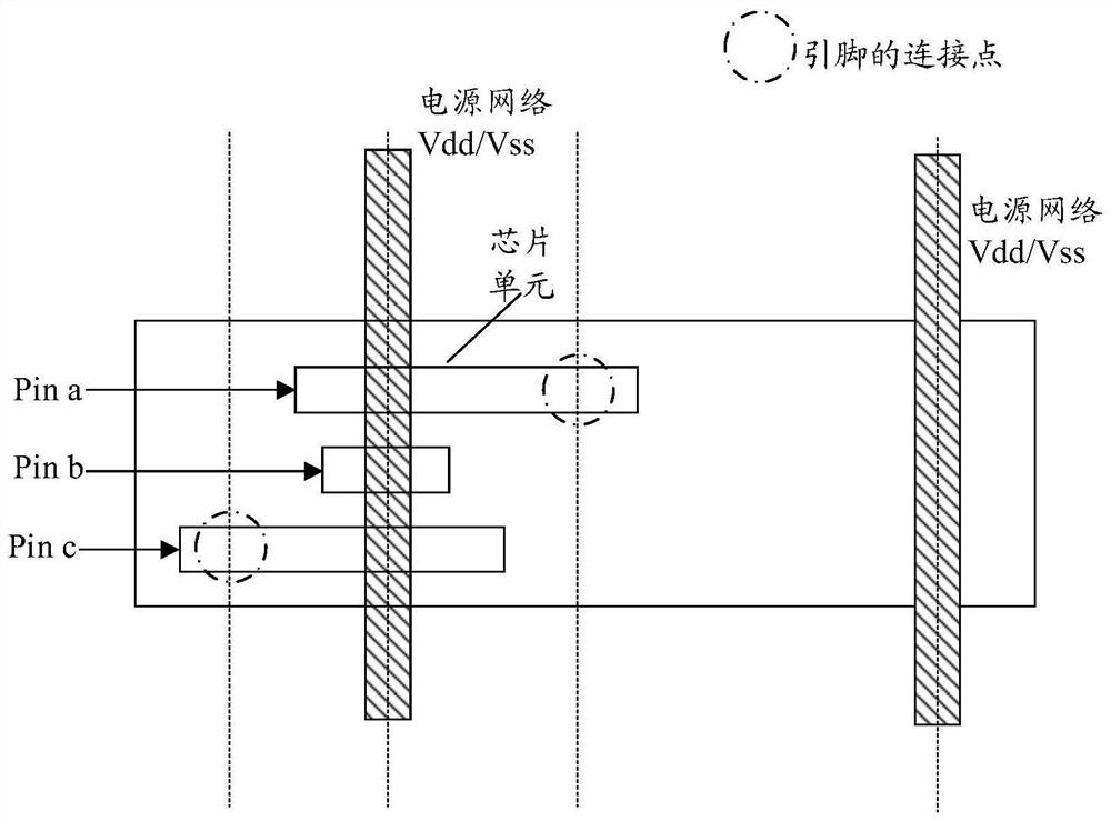
[0075] In the related technology, with the shortening of the semiconductor manufacturing process, the power supply network becomes denser and the pins of the chip unit become shorter and shorter. When wiring the chip unit, if the chip unit and the power supply network are arranged on different circuit layers , the connection point of the pins of the chip unit may be covered by the power network. figure 1 is a schematic diagram of the connection points of the pins of the chip unit in the related art, taking the chip unit as a standard unit as an example, such as figure 1 As shown, one connection point of the pin Pin a of the standard unit is covered by the power supply network Vdd or the power supply network Vss, and the other connection point is not covered by the power supply network Vdd or the power supply network Vss; th...


PUM


Abstract

The invention discloses a wiring method and device, equipment and a storage medium. The method comprises the following steps: determining at least two chip units to be wired; selecting at least one first chip unit from the at least two chip units to be wired; wherein each first chip unit is a chip unit of which all connection points of pins are covered by a power supply network; determining a wiring constraint condition between the at least one first chip unit and a corresponding power supply network to obtain at least one wiring constraint condition; and according to the at least one wiring constraint condition, wiring the at least one first chip unit, so that at least one connection point of a pin of the at least one first chip unit is not covered by a power supply network.

Description

technical field [0001] The invention relates to semiconductor technology, in particular to a wiring method, device, equipment and storage medium. Background technique [0002] With the rapid development of intelligent electronic devices, chip units in intelligent electronic devices are closely related to semiconductors. With the shortening of the semiconductor manufacturing process, the power supply network is becoming more and more dense, and the pins of the chip unit are getting shorter and shorter. When wiring the chip unit, if the chip unit and the power supply network are distributed on different circuit layers, it may be When the connection points of the pins of the chip unit are covered by the power network, the user needs to manually change the layout. Due to the large number of changes, the overall wiring speed is affected. [0003] Therefore, continue to find a technical solution to increase the wiring speed. Contents of the invention [0004] In view of this, ...

Claims


Application Information

Patent Timeline
Patent Type & Authority Applications(China)
IPC IPC(8): G06F30/3947H01L27/02G06F111/04
CPCG06F30/3947G06F2111/04H01L27/0207
Inventor 刘君
Owner GUANGDONG OPPO MOBILE TELECOMM CORP LTD
Why Eureka
Try Eureka