Array substrate, display panel, and display device thereof

a display panel and substrate technology, applied in the field of display technology, can solve the problems of affecting the picture quality, affecting the uniform width of the display region, and different signal delay between the gate lines having different lengths

Active Publication Date: 2020-05-05
SHANGHAI AVIC OPTOELECTRONICS
View PDF21 Cites 7 Cited by
  • Summary
  • Abstract
  • Description
  • Claims
  • Application Information

AI Technical Summary

Benefits of technology

[0064]In the array substrate, the display panel and the display device provided by the present disclosure, the second trace portion of the irregular gate line may be configured to have the line width smaller than the first trace portion of the irregular gate line. In other words, the second trace portion may be configured to have the line width smaller than the regular gate line, such that the resistance of the second trace portion may increase. Accordingly, the load capacitance of the irregular gate line may be increased, and the regular gate line may have the same load capacitance as the irregular gate line, which may improve the uniformity of the display panel, and improving the display performance of the display panel.

Problems solved by technology

Along a length direction of a gate line, a width of the display region is not uniform.
The load capacitance of the gate line affects a signal transmission time, which results in different signal delay between the gate lines having different lengths.
Different signal delay may degrade picture quality.

Method used


Image

  • Array substrate, display panel, and display device thereof
  • Array substrate, display panel, and display device thereof
  • Array substrate, display panel, and display device thereof

Examples


Embodiment Construction

[0020]Reference will now be made in detail to exemplary embodiments of the disclosure, which are illustrated in the accompanying drawings. Wherever possible, the same reference numbers will be used throughout the drawings to refer to the same or the alike parts. The described embodiments are some but not all of the embodiments of the present disclosure. Based on the disclosed embodiments, persons of ordinary skill in the art may derive other embodiments consistent with the present disclosure, all of which are within the scope of the present disclosure.

[0021]Similar reference numbers and letters represent similar terms in the following Figures, such that once an item is defined in one Figure, it does not need to be further discussed in subsequent Figures.

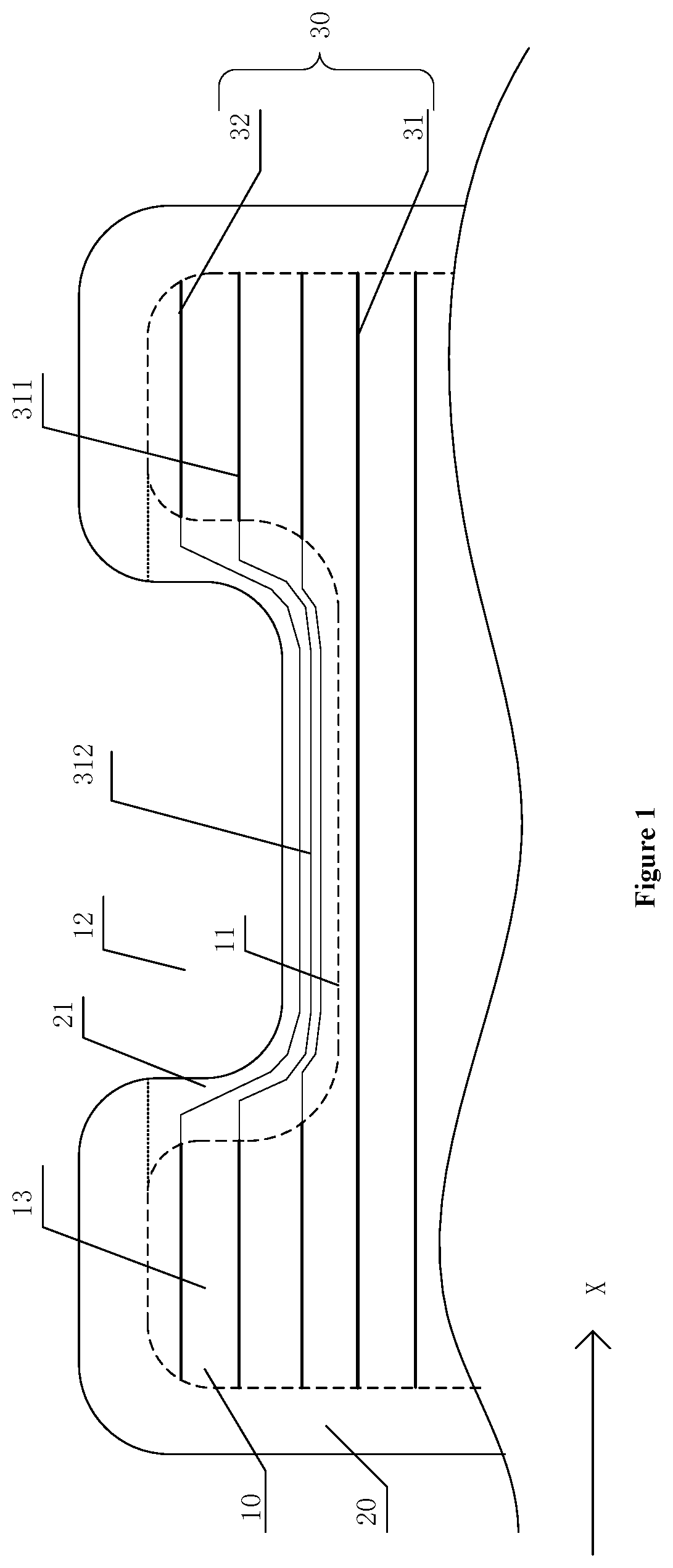
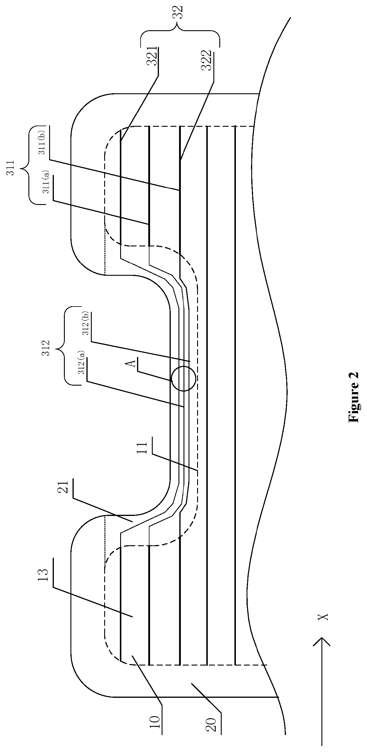
[0022]FIG. 1 illustrates a schematic diagram of a local structure of an exemplary array substrate consistent with disclosed embodiments of the present disclosure. Referring to FIG. 1, the array substrate may include a display region ...


PUM

PropertyMeasurementUnit
widthaaaaaaaaaa
widthaaaaaaaaaa
widthaaaaaaaaaa

Abstract

An array substrate, a display panel, and a display device are provided. The array substrate includes a display region and a non-display region surrounding the display region. The array substrate also includes a plurality of gate lines. The plurality of gate lines include a plurality of regular gate lines and at least one irregular gate line. The plurality of regular gate lines are disposed in the display region and extended along a first direction. The at least one irregular gate line includes at least one first trace portion and a second trace portion electrically connected to each other. The at least one first trace portion has a same line width as a regular gate line of the plurality of regular gate lines, and the second trace portion has a line width smaller than the at least one first trace portion.

Description

CROSS-REFERENCES TO RELATED APPLICATIONS[0001]This application claims the priority of Chinese patent application No. 201810260555.8, filed on Mar. 27, 2018, the entirety of which is incorporated herein by reference.FIELD OF THE DISCLOSURE[0002]The present disclosure generally relates to the field of display technology and, more particularly, relates to an array substrate, display panel and display device thereof.BACKGROUND[0003]In daily life, more and more rich visual information are utilized by people and, thus display technology plays a very important role in today's human society. With the development of science and technology, display technology is rapidly advancing toward narrow borders and full display. In an existing display panel, a display region has a non-rectangular shape. Along a length direction of a gate line, a width of the display region is not uniform. Thus, the gate lines in the display region in the display panel will have different length and, accordingly, corres...

Claims


Application Information

Patent Timeline
Patent Type & Authority Patents(United States)
IPC IPC(8): G06F3/044H01L27/12
CPCH01L27/124G06F3/044G09G2320/0233G02F1/136286H10K59/131G06F3/0443G06F3/0412G06F3/04164
Inventor WANG, TINGHAIJIN, HUIJUNQIN, DANDANFEI, RILIXIE, YING
Owner SHANGHAI AVIC OPTOELECTRONICS
Why Eureka
Try Eureka